A wireless, low-profile remake of the handwired Diamond (1333+2 per half). The layout and goals are mine; Claude, working in Claude Code, generated the PCB, the printed case and every check as code.
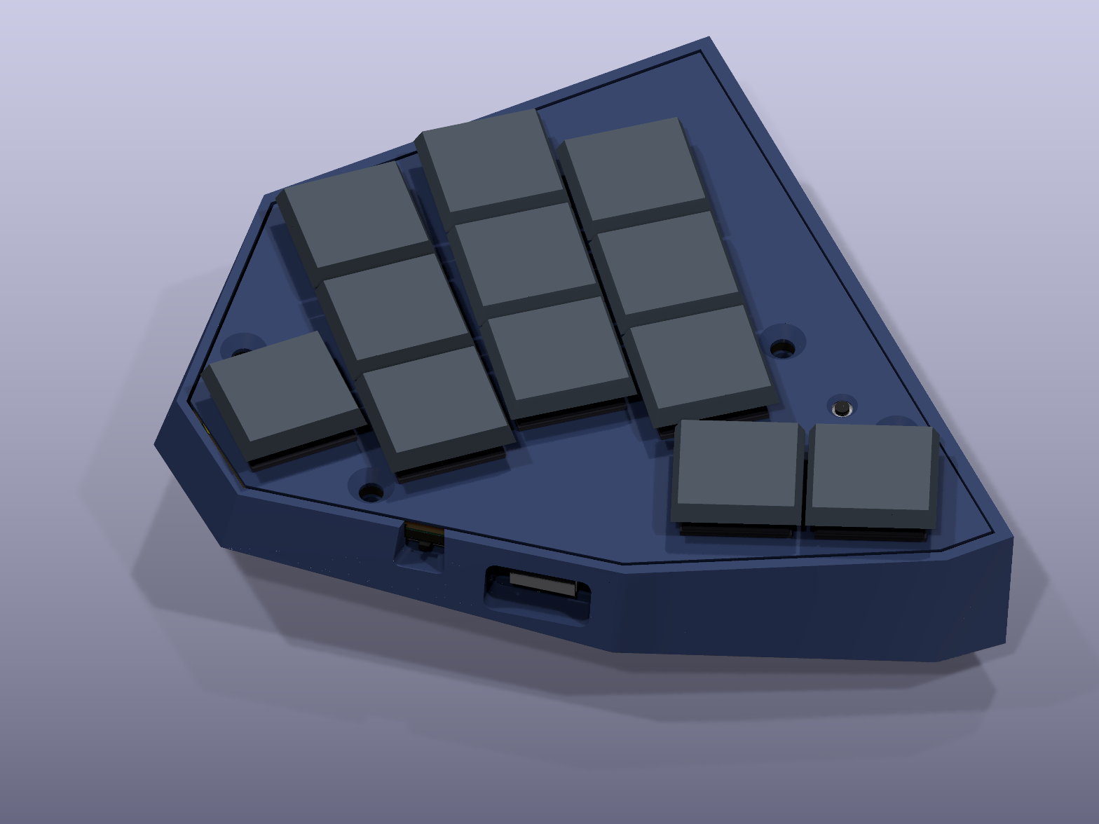
The board
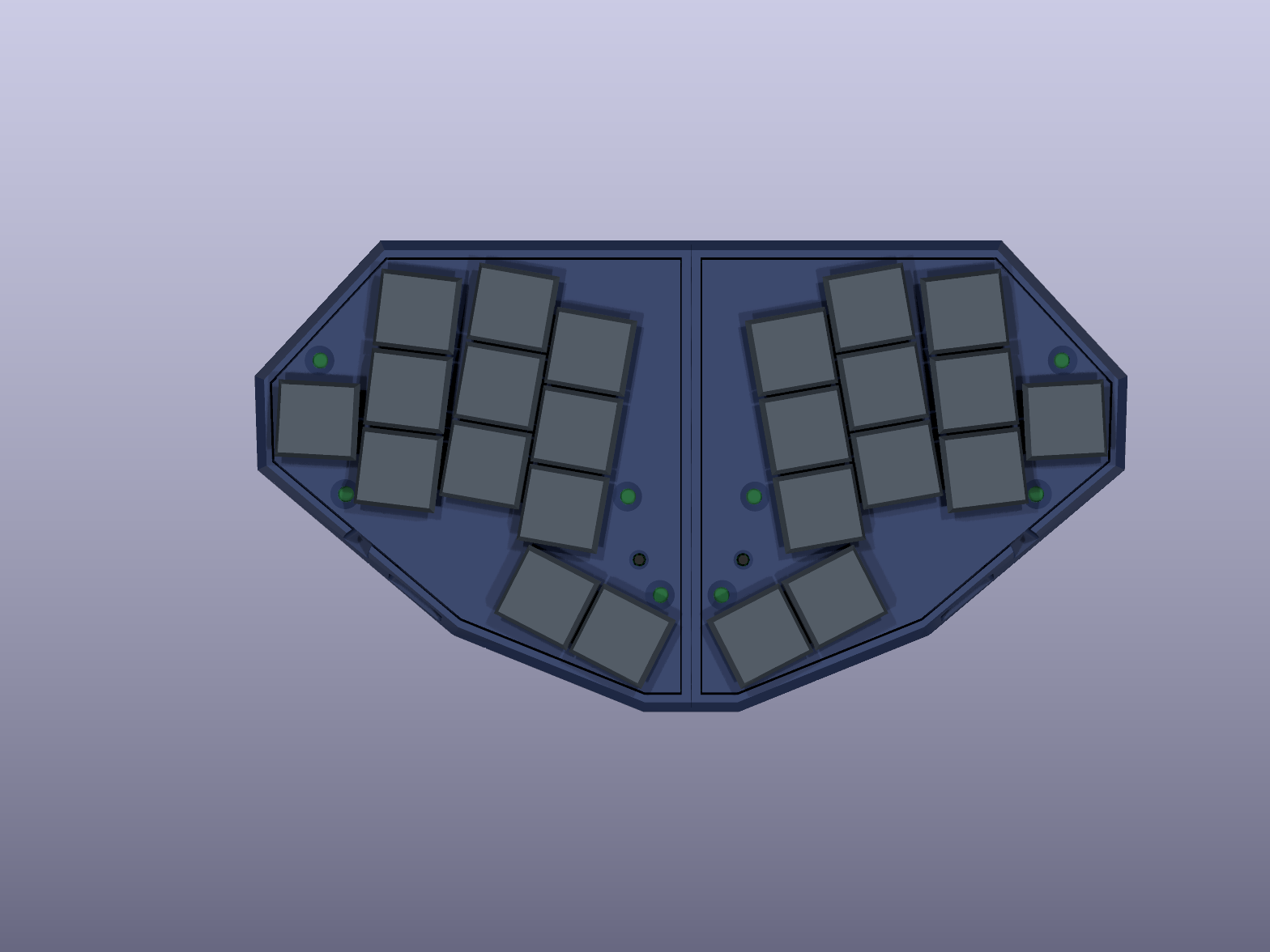
| Keys | 24 Choc v1 hot-swap, all 1u: 3×3, a pinky key and two thumbs per half |
|---|---|
| Wiring | Diodeless, one pin per key: 11 XIAO edge pins plus the NFC1 pad |
| Controller | One XIAO-sized nRF52840 per half, either the Seeed XIAO nRF52840 or the NologoTech Super52840. Same board, same ZMK firmware |
| Power | 500 mAh LiPo (nominal 7 × 20 × 40 mm) on a JST PH socket, and an MSK-12C02 slide switch beside the USB-C port |
| PCB | 87.6 × 92.3 mm, 2 layers, one reversible design for both halves |
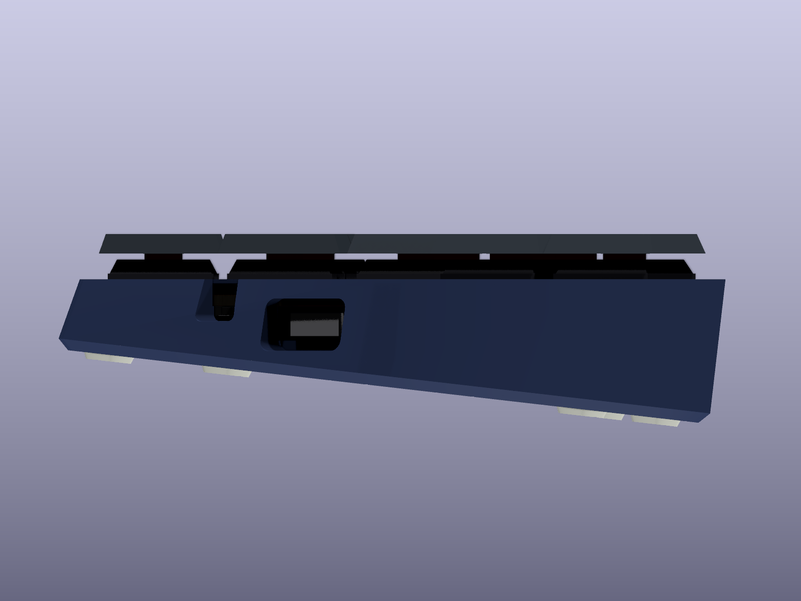
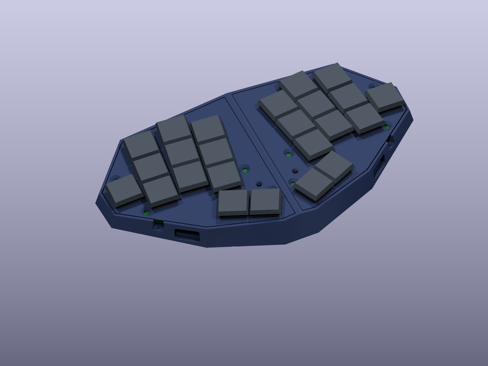
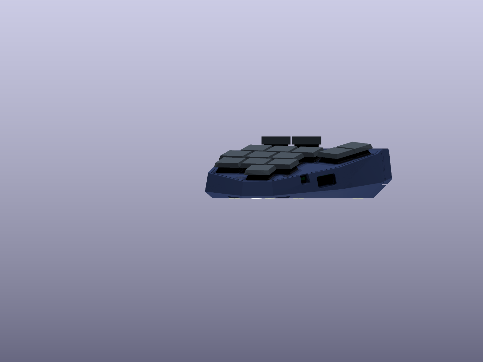
| Case | Solid printed base tented 6.6° (20.4 mm at the seam, 10.5 mm at the outer edge), with a 1.2 mm top plate |
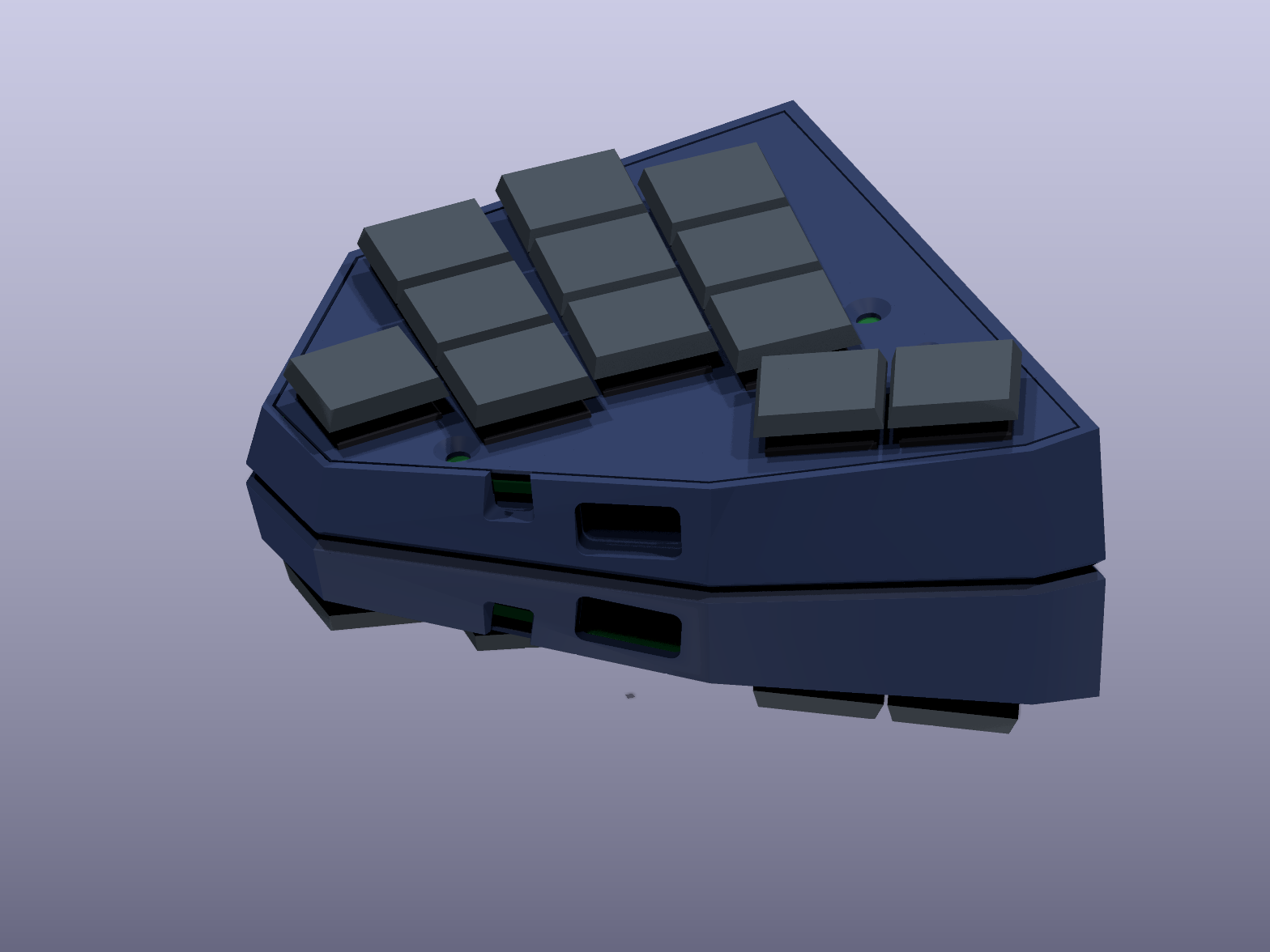
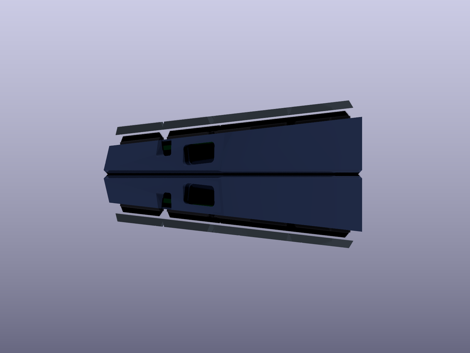
| Extras | Magnets to join the halves or stack them for travel, interleaving anti-slip pads, a reset button under a cone hole in the plate |
| Assembly | Soldering iron only: no paste, no hot air |
The reversible trick
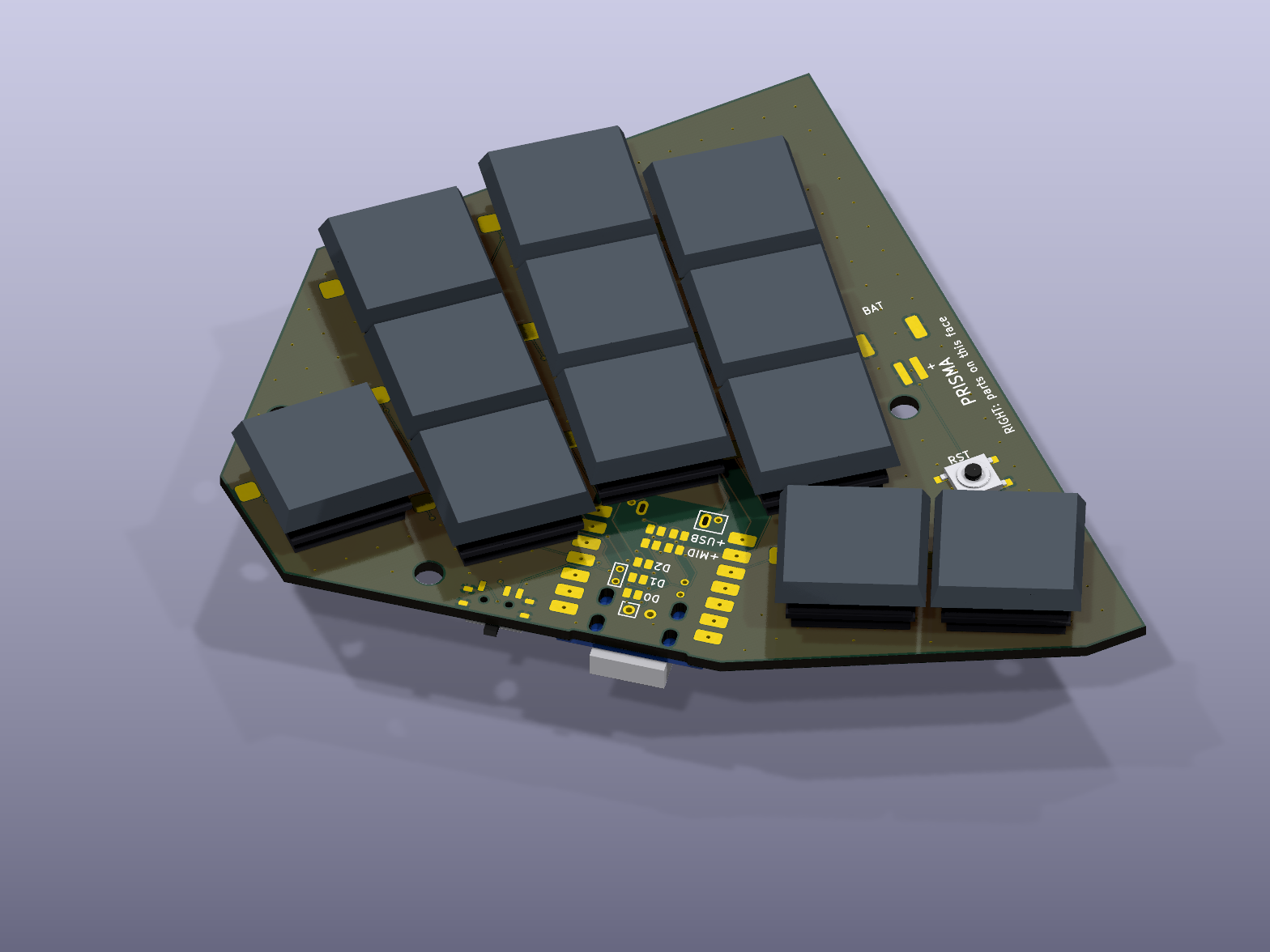
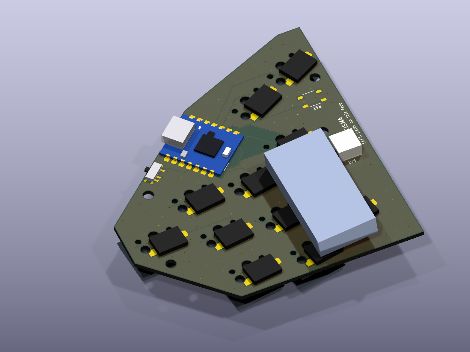
The left half carries its parts on the back face; the right half is the same board flipped, with parts on the front. Flipped, the module's pins land mirrored: the left half's D0, D1 and D2 become VBUS, GND and 3V3. Solder jumpers route those three to their keys, and you bridge only the set on the face without the module.
The module's underside pads (battery, 12th key, reset) are reached through plated holes filled with solder from the other face, so everything stays iron-friendly. The reset pad sits under the module's GND pad on the opposite mount, so each half's reset hole has its own net and reaches only that half's button.
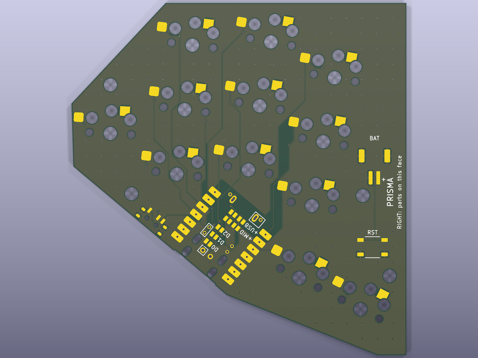
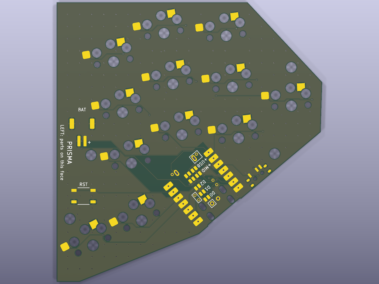
XIAO or Super52840
Both modules have the same 14 edge pins on the same nRF52840 pins, so layout, case, plate and firmware are shared. Underneath they differ. Their battery pads sit in the same two spots but swapped, so a selector on the switch face picks which hole is +: bridge +MID or +USB. The Super52840's pads were measured from photos against the 2.54 mm pin pitch.
| Seeed XIAO nRF52840 | NologoTech Super52840 | |
| Battery + | The pad nearer the middle: bridge +MID | The pad nearer the USB end: bridge +USB |
| 12th key | NFC1 pad (P0.09) | P0.09 in a row of nine extra GPIO pads: a hole under each, on one net |
| Reset | Test pad | Same place |
| USB-C | Surface-mount | Legs through its board, cleared by holes; sticks out 0.8 mm further, into the case's recess |
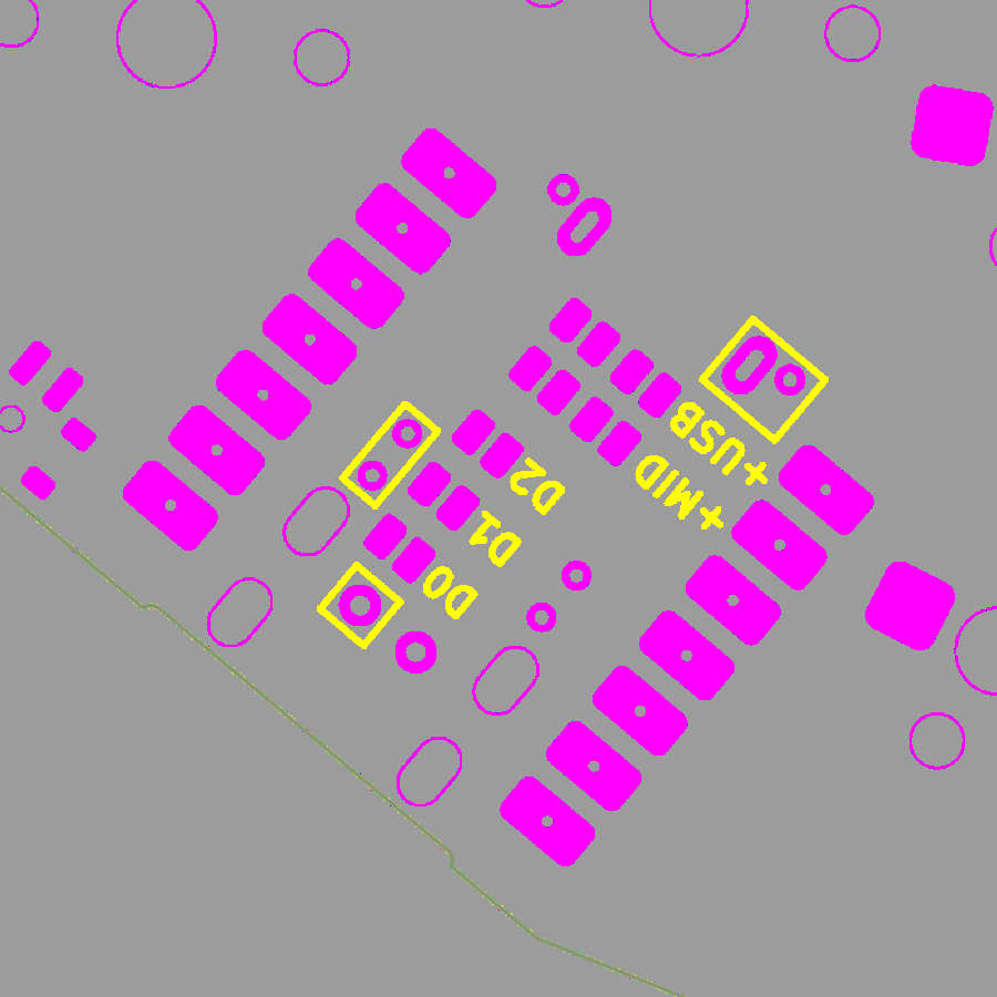
+MID / +USB selector, the fill holes.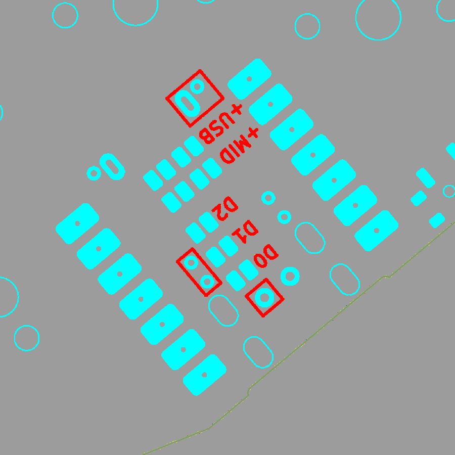
Base, plate, two ways to join
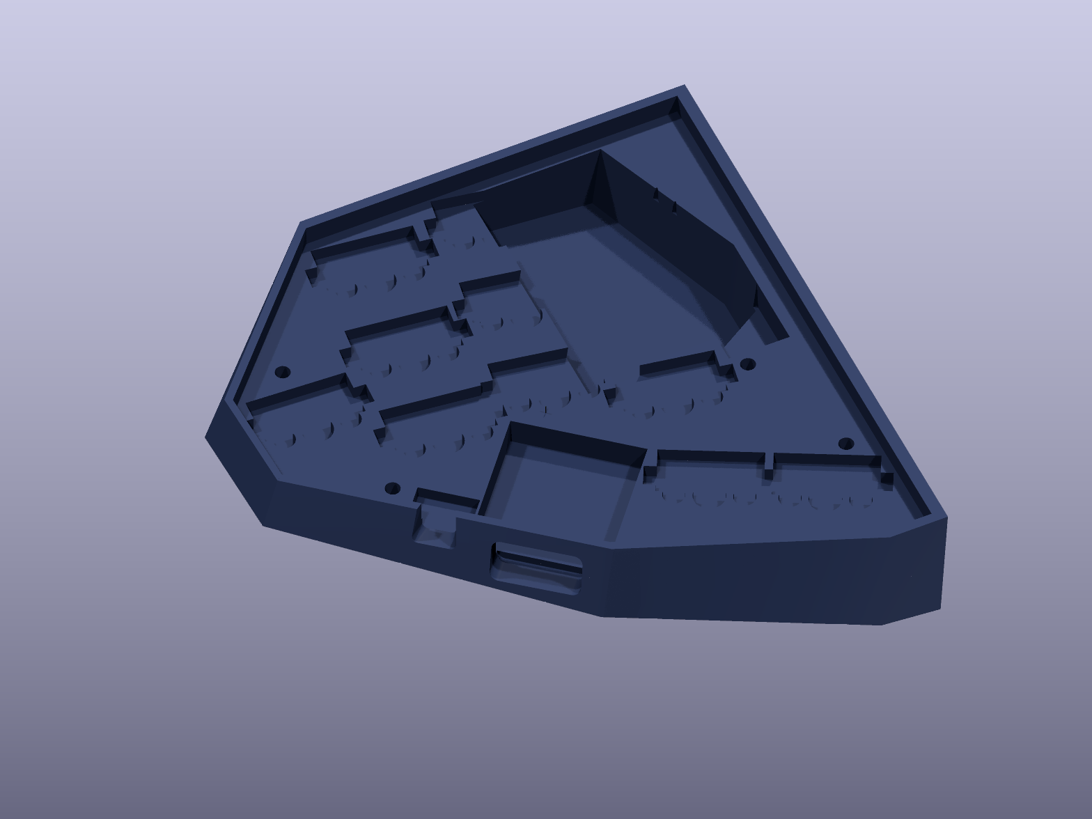
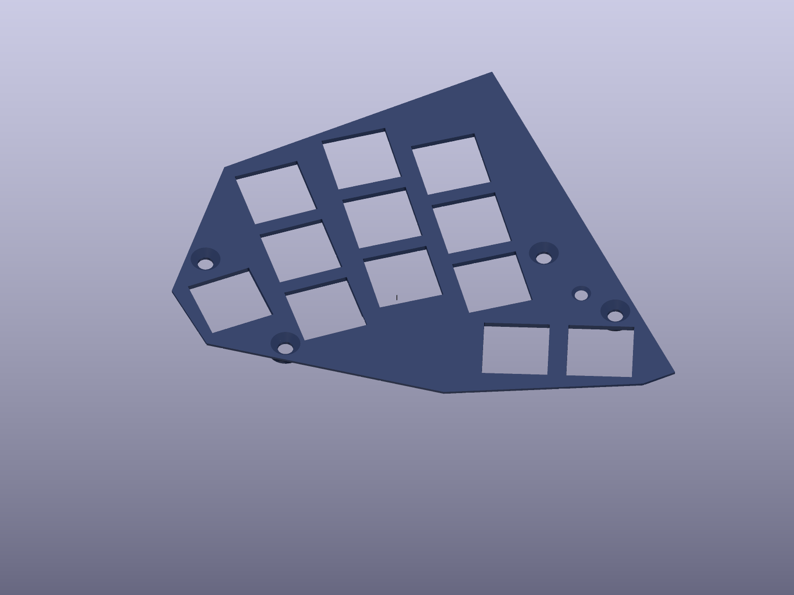
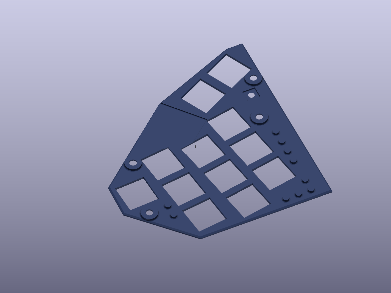
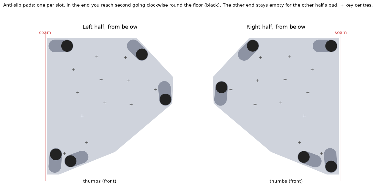
A solid base with a pocket per part, a top plate on top, and anti-slip pads that sit in different ends of each slot so they interleave when the halves are stacked.
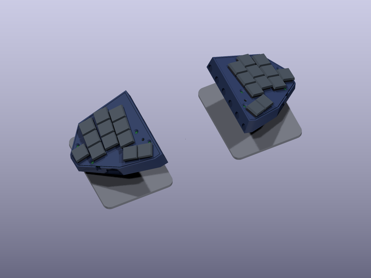
Independent tenting
Use two steel phone stands: magnetic attraction on the actual supports has been tested. The half's three stand magnets, 120° apart on a 44 mm circle around its estimated centre of gravity, pull directly on the tilting platform (not the base); no extra discs are needed. All foot positions lie at least 11.55 mm outside the centred 54 mm contact circle, so they do not create an air gap there. Keep magnets flush and faces free of glue. The 54 mm minimum leaves only 1 mm radial magnet-edge margin; prefer about 60 mm if the real platform still clears the feet and obstructions. Aluminium and nonmagnetic stainless steel are unsuitable. The estimated gravity projection stays inside the contact triangle through 35° of tilt, but slip, peel and typing-load retention still need testing.
A dock for a phone stand
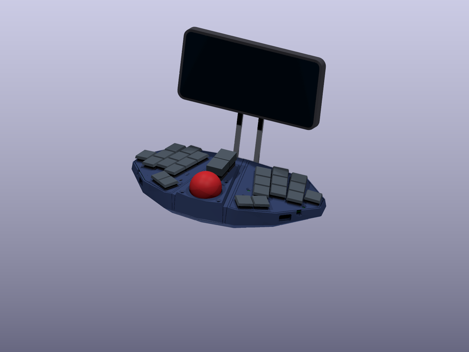
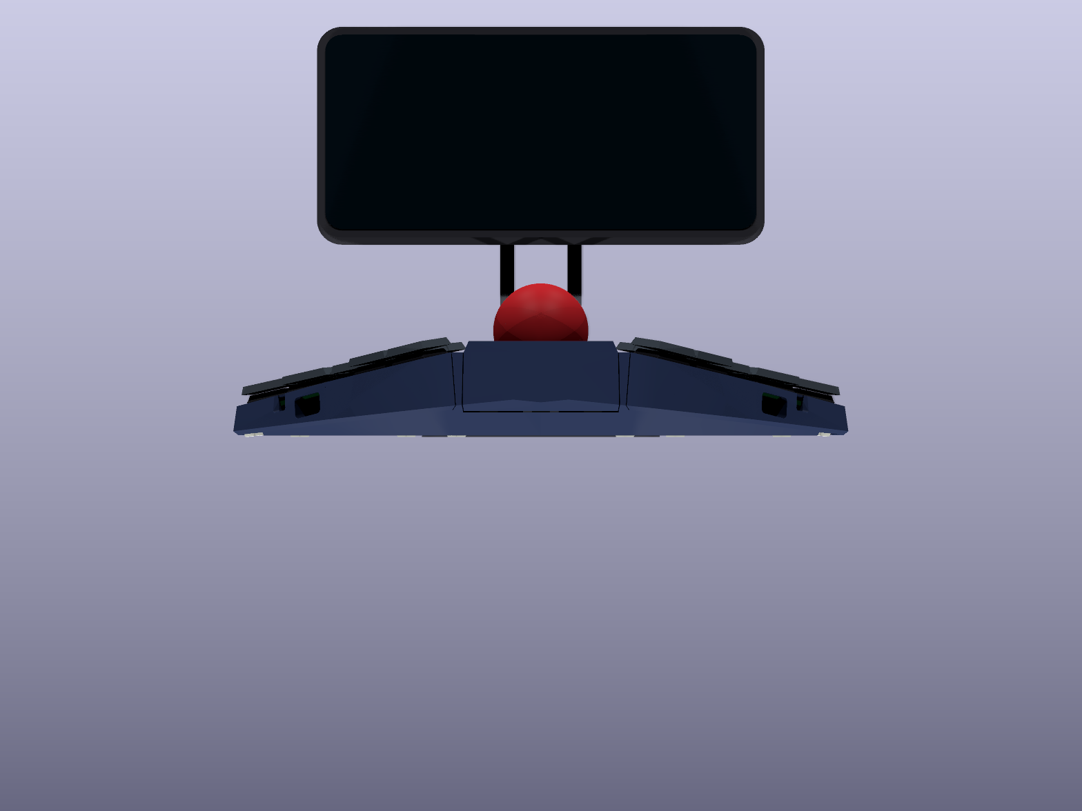
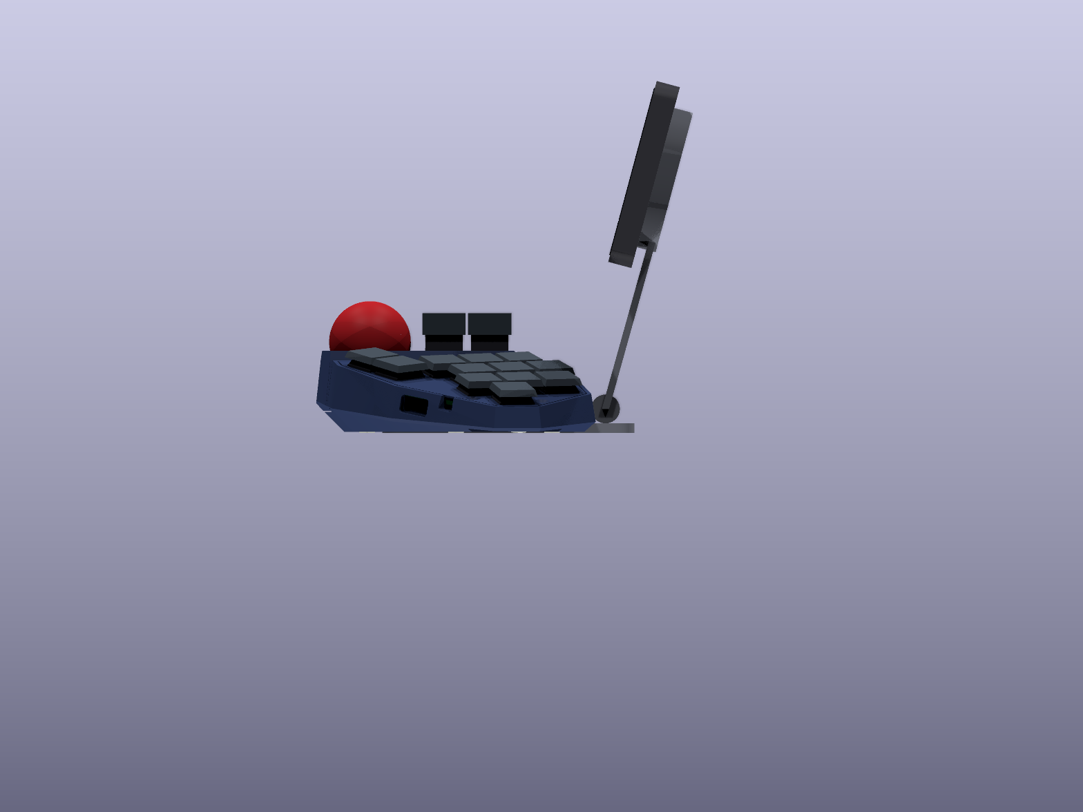
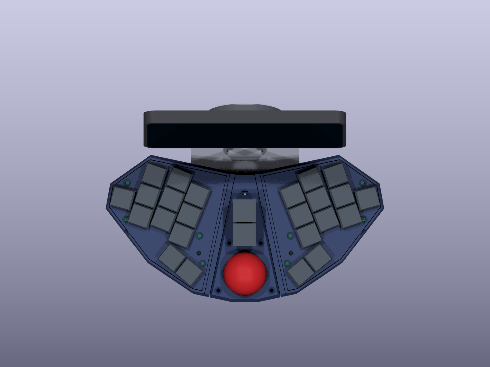
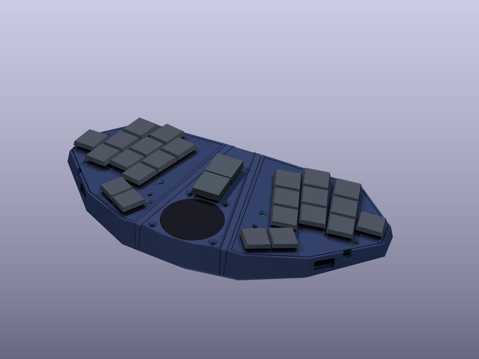
A phone on a Ugreen folding stand is the computer and the screen. The dock is one printed part that holds both halves around it. It sits over the stand's base, which stays on the desk on its own feet and carries the phone; behind the dock the base is bare, its hinge half a millimetre off the halves and the spine. Without the stand, the dock is a sturdier, more tented unibody.
It continues the halves' 45° bottom facets down to the desk, with 12° of splay and 5.70° of extra tent (about 12.3° in all). The middle is a front-opening drawer for a trackball, a trackpad or a solid placeholder, which slide out horizontally. At the back, each insert extends only its top into a 45° hood over a matching dock support, 0.4 mm clear.
Everything is held by the same 8 × 1.5 mm N52 discs. Six wing magnets mate six of each half's seven floor magnets, and three more per side pass through 0.6 mm inner skins to the insert, so every join attracts: half → dock → insert. One more disc in the drawer floor grips a module from below, and three pairs attach the dock to the Ugreen base. The rear stays free for USB and the power switch. The dock measures 199.0 × 111.3 × 29.8 mm (about 83 cm³).
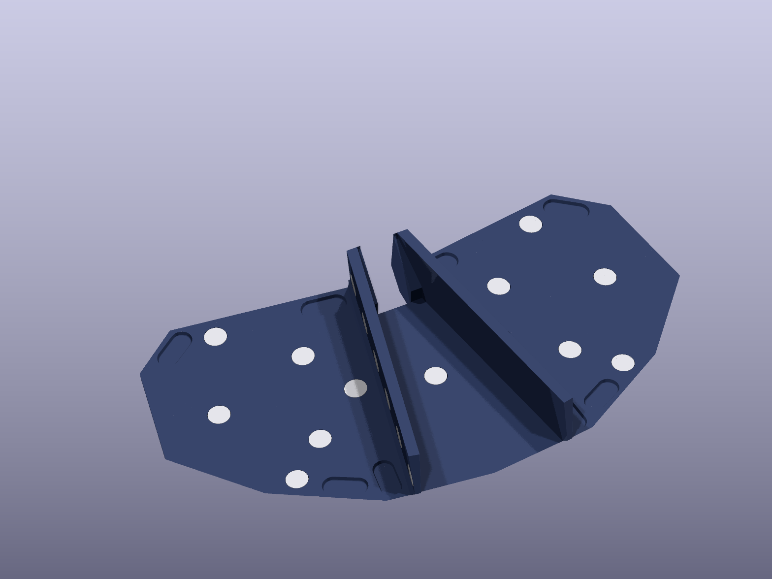
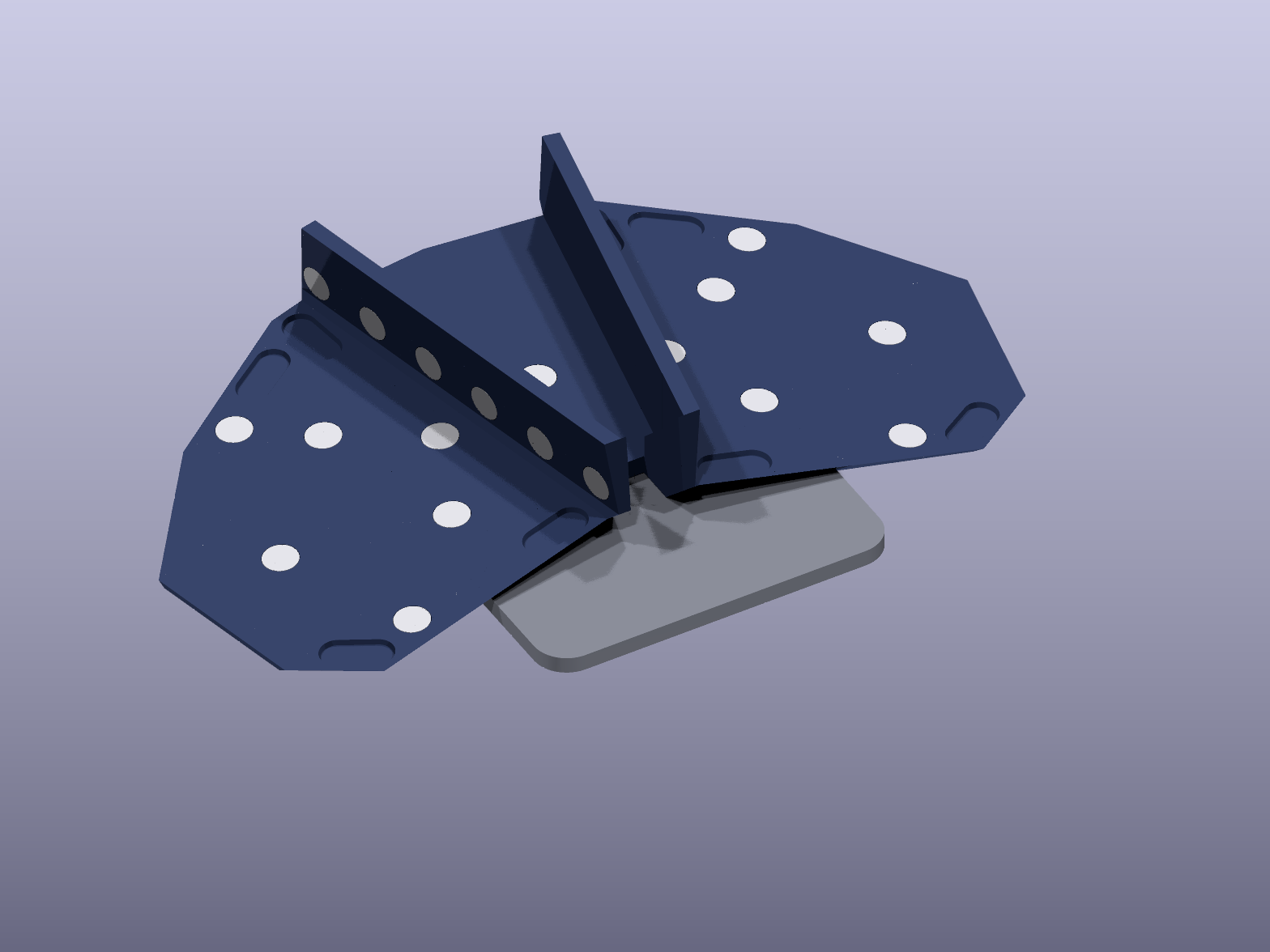
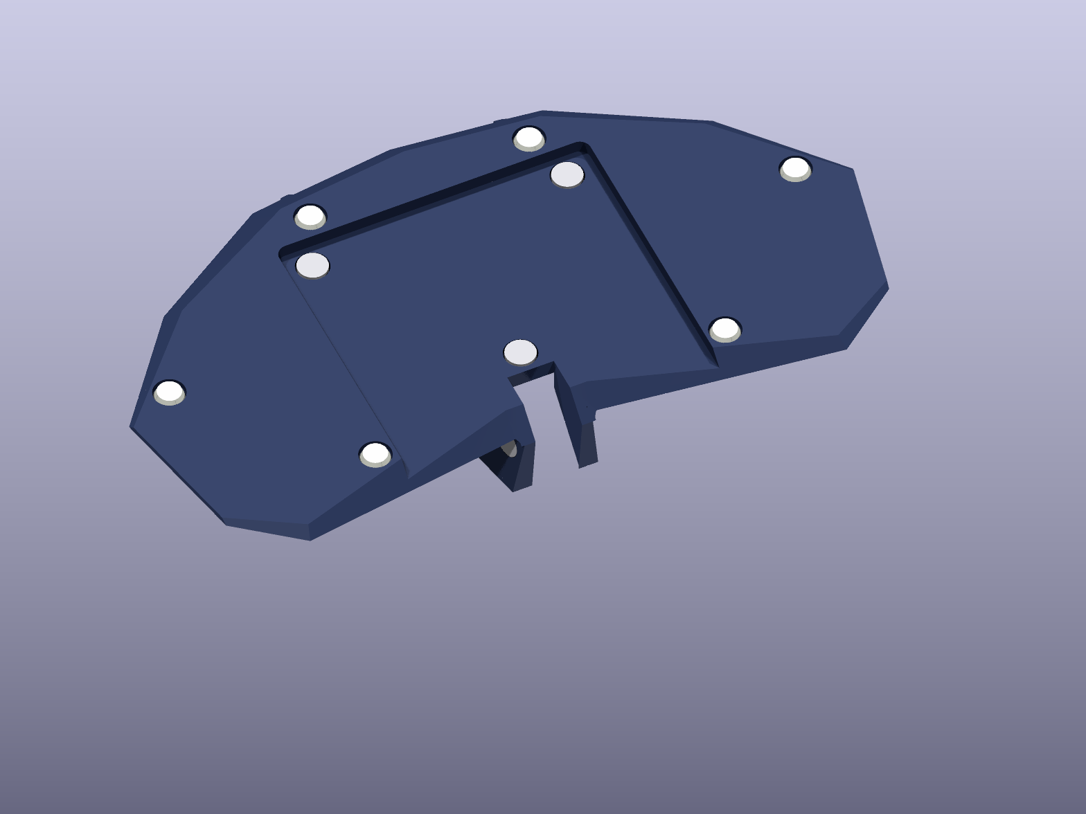
A trackball or a trackpad, in the drawer
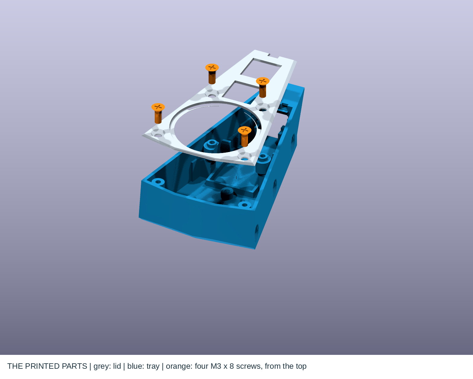
Two ZMK pointing modules that slide into the dock's drawer or snap onto a half on the desk. They are built like a half: a tray, a lid, and the same M3 × 8 flat-head screws from the top. Tray, main board, battery, power switch and reset button are shared. The controller, a nice!nano v2 or a plain XIAO nRF52840, sits on its own small board under the main board.
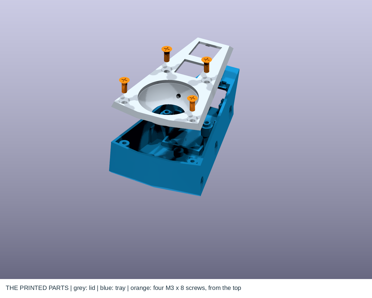
Three side magnets per side use every other position in the halves' six-magnet row, and one disc in the module's floor mates with the drawer floor. To remove a module, push its rear hood forwards through the dock's rear passage.
Trackball: a 34 mm ball and PMW3610 sensor, with two MX or Choc v1 hot-swap keys on one shared PCB. Populate one socket family and print the matching lid.
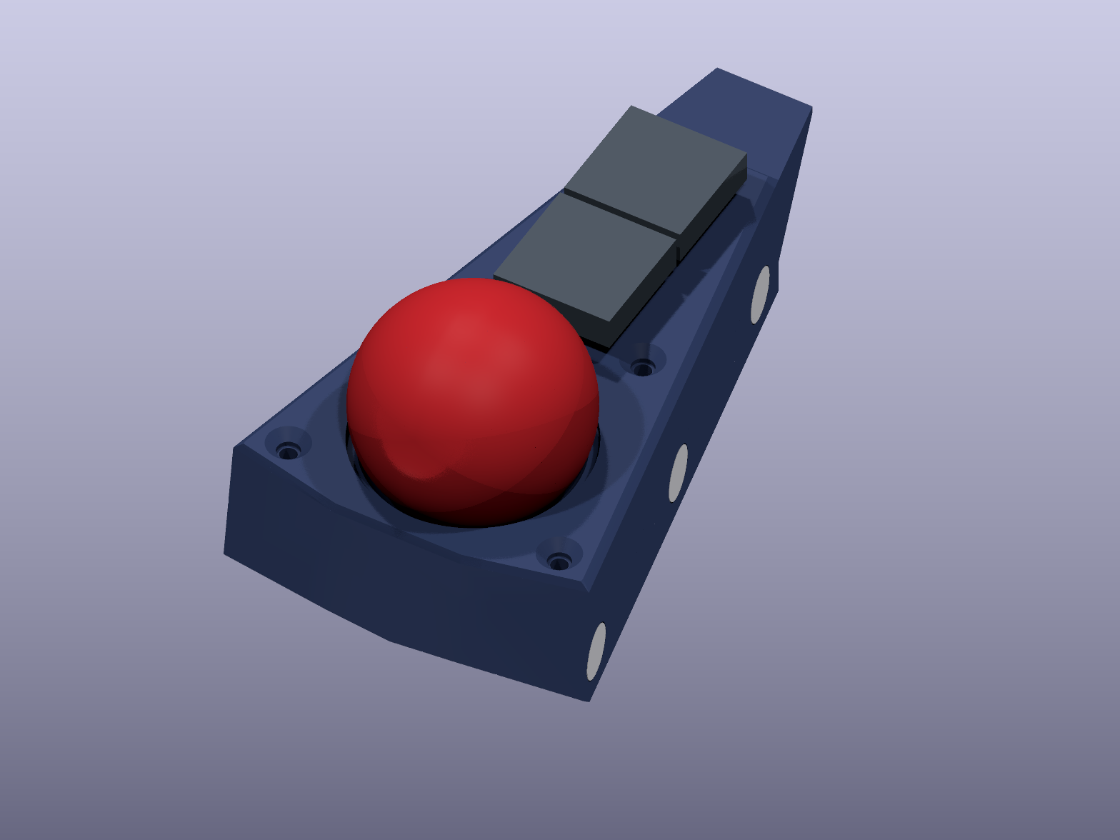
Trackpad: a 40 mm Cirque in the lid, with its supplied I²C breakout and flat cable. Four wires run from the main board to the breakout and a separate DR wire to the Cirque's underside. Space is reserved for the breakout and cable with no printed holder; check your kit's dimensions against the build guide.
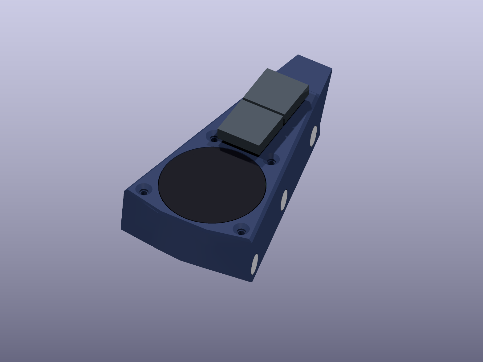
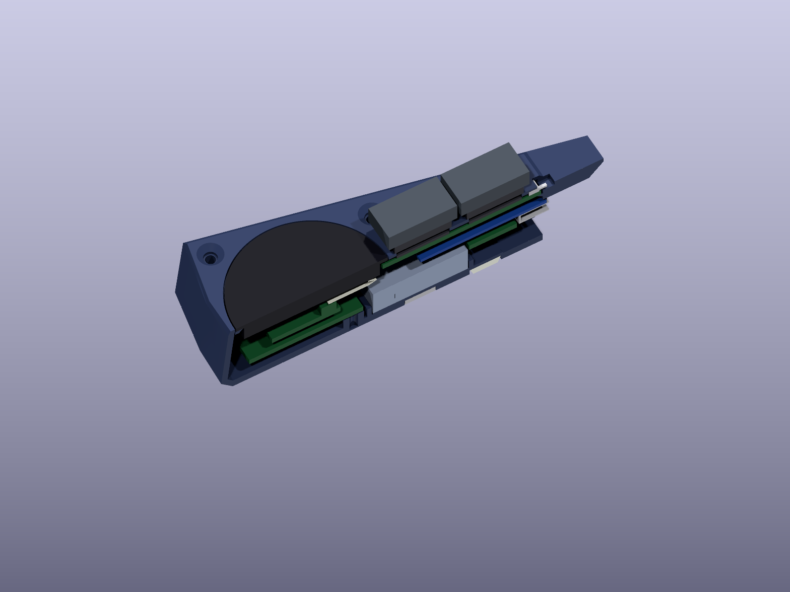
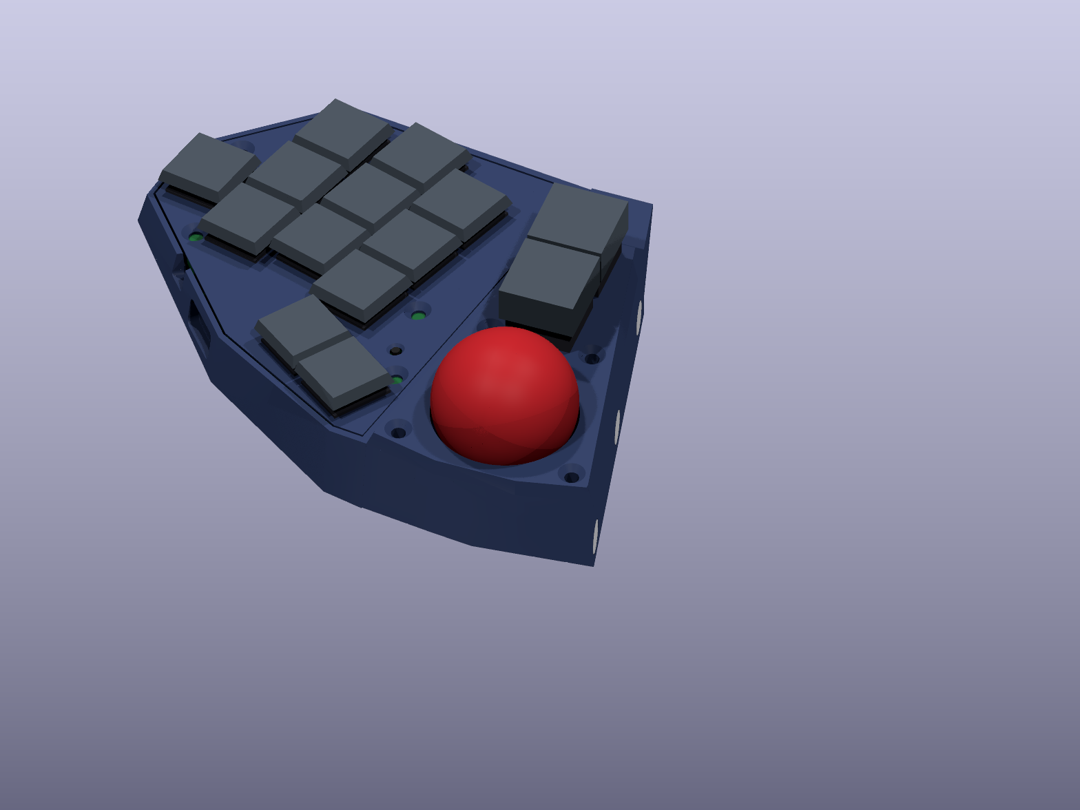
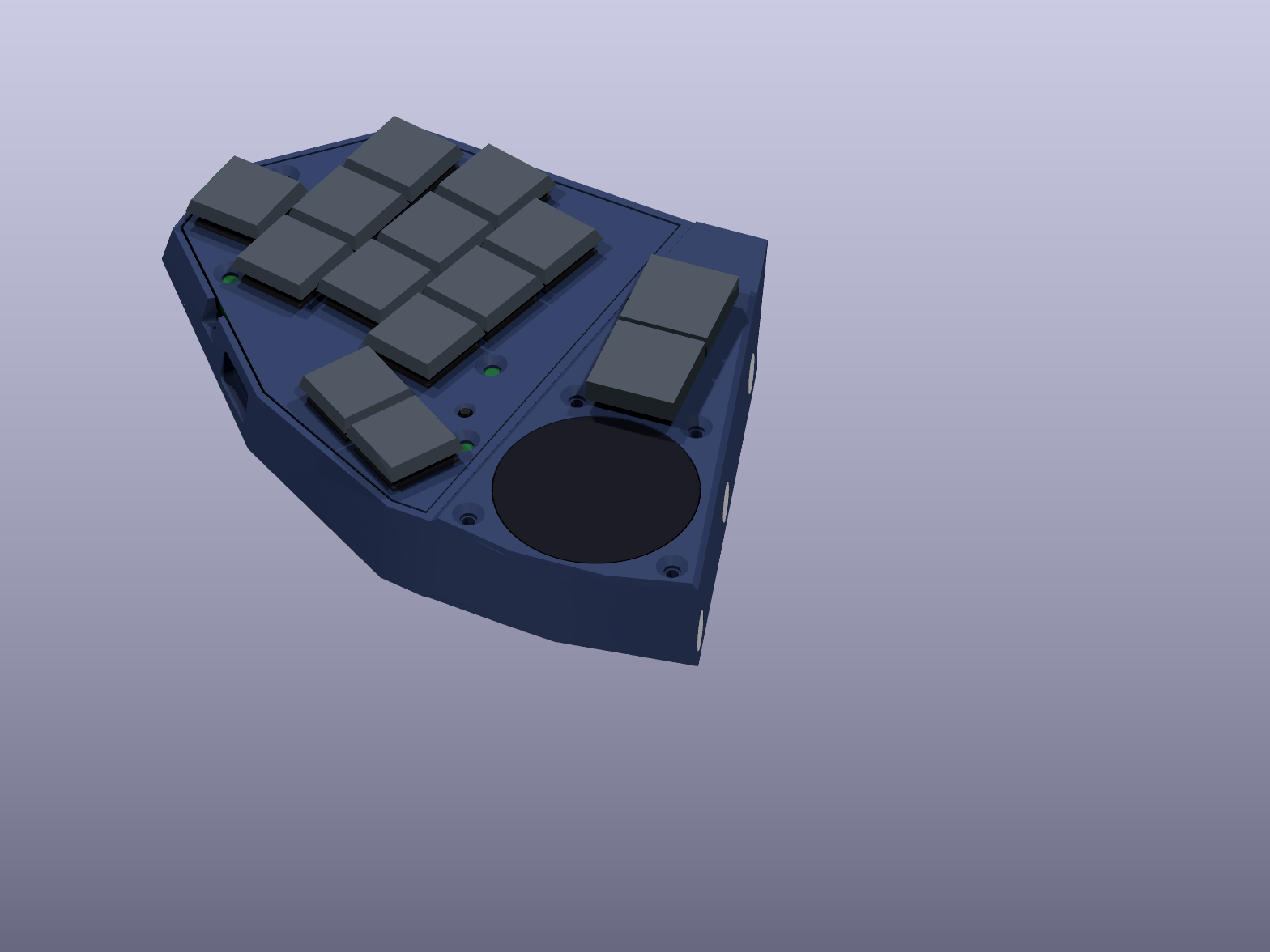
USB-C, seated
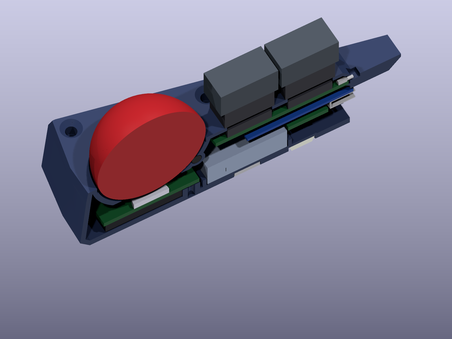
The port is flush with the module's back with nothing beneath it, and the dock's 12.8 mm rear passage leads straight to it. The renders use an illustrative 12.35 × 6.5 mm plug and cable.
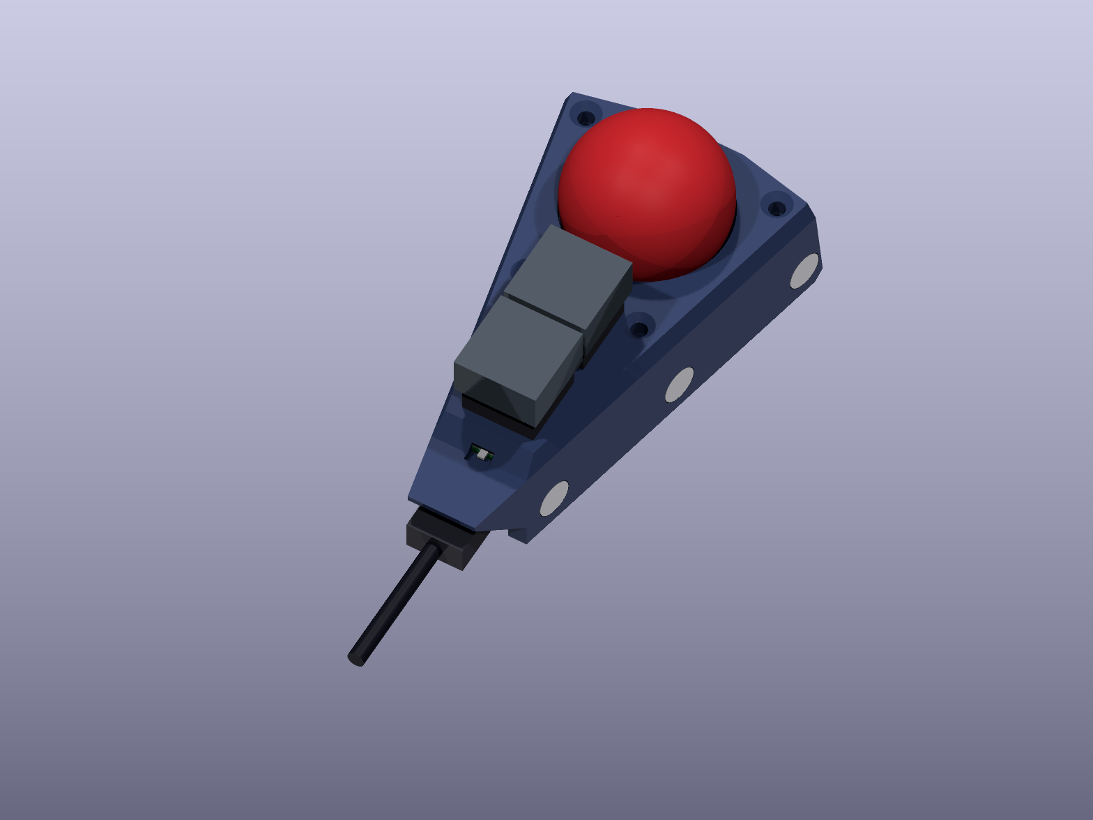
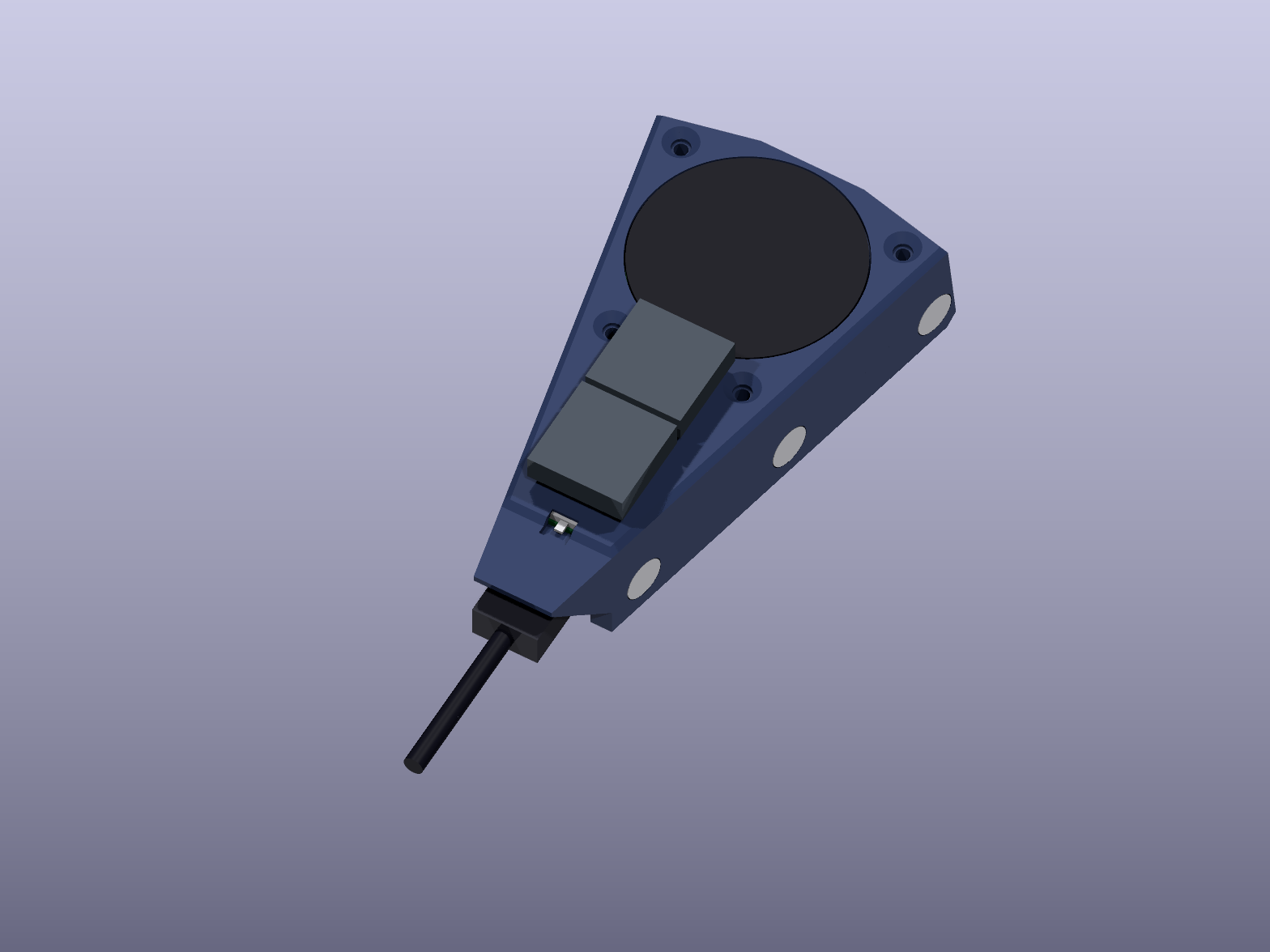
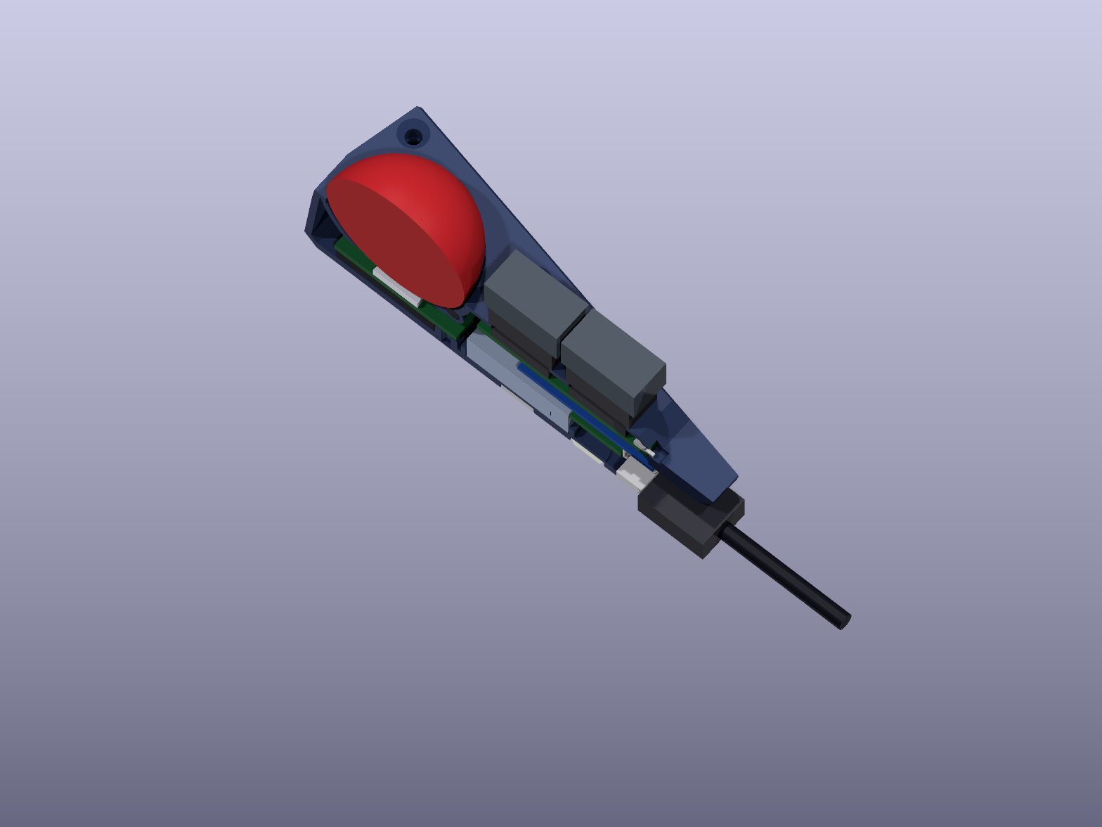
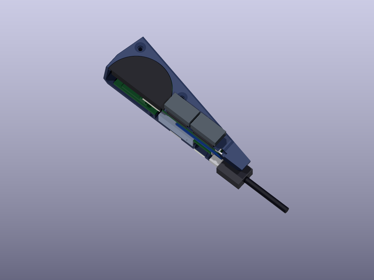
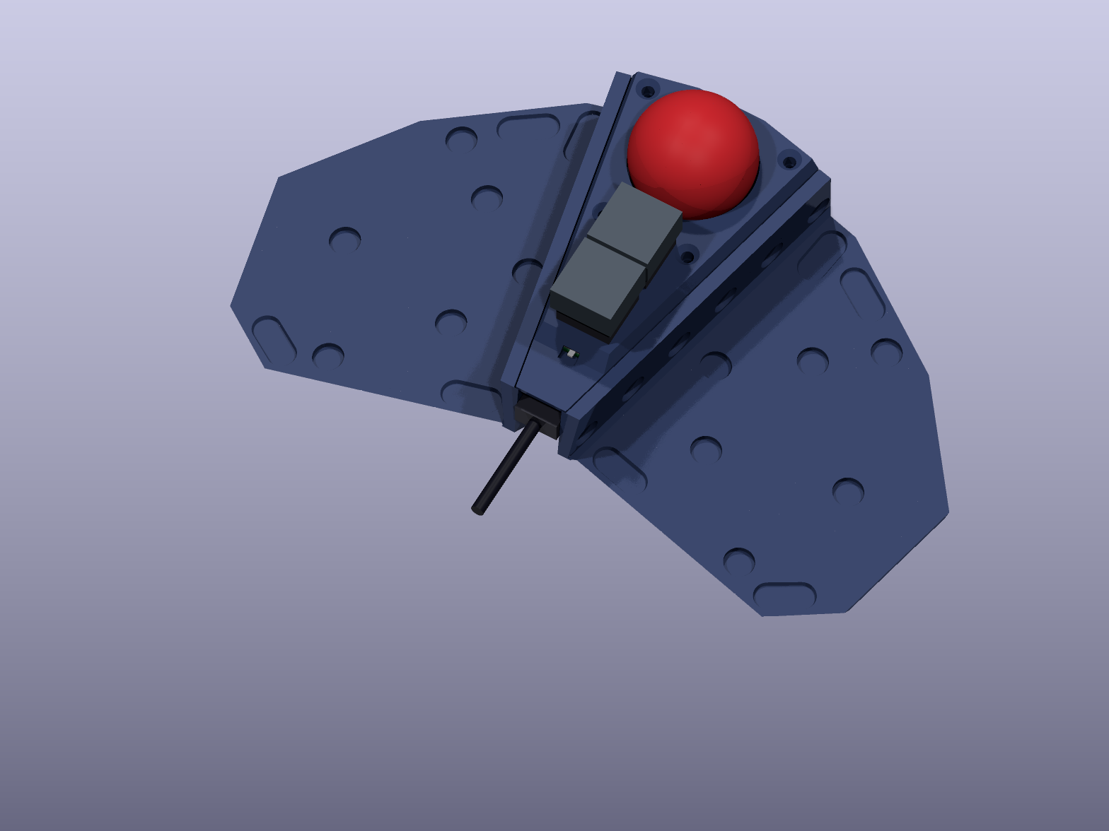
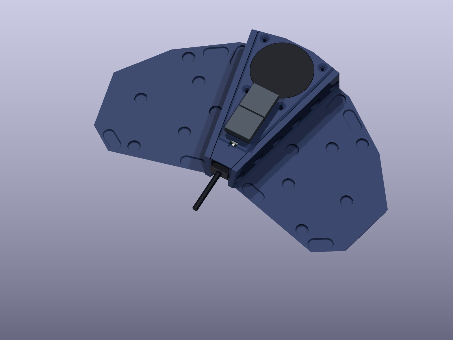
One panel, either controller
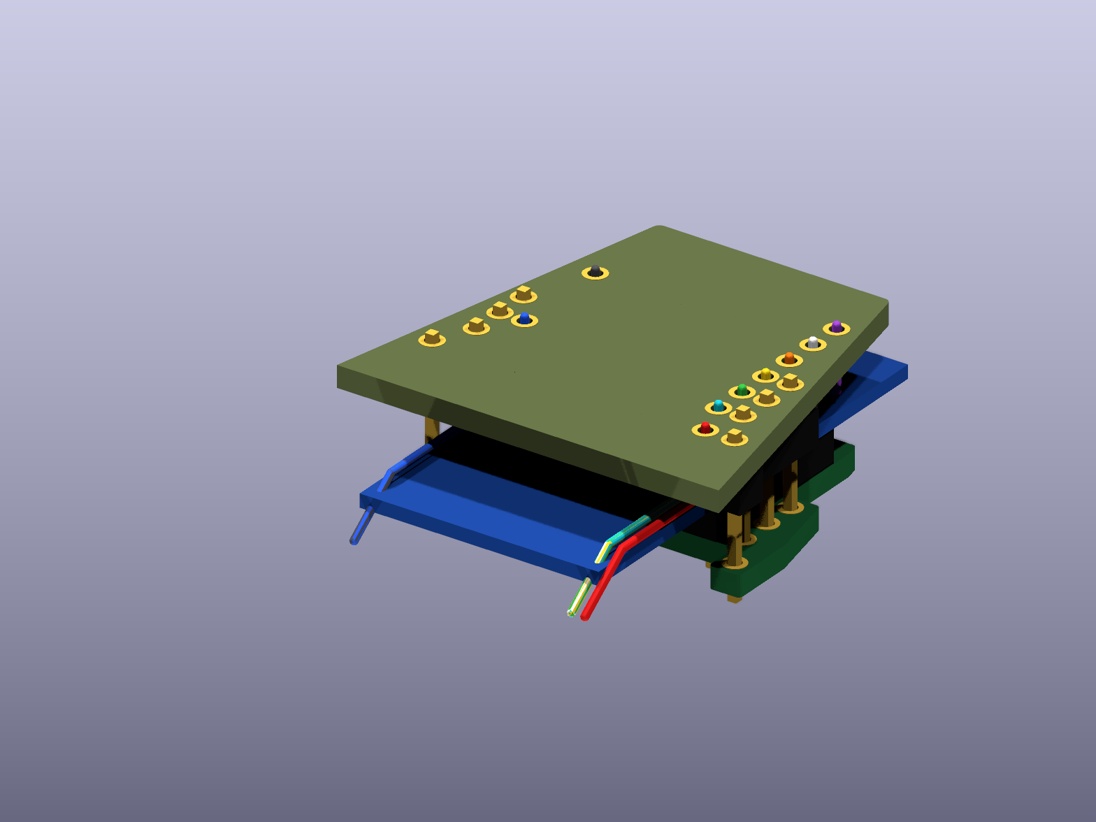
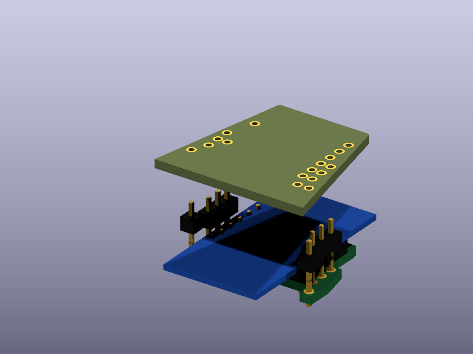
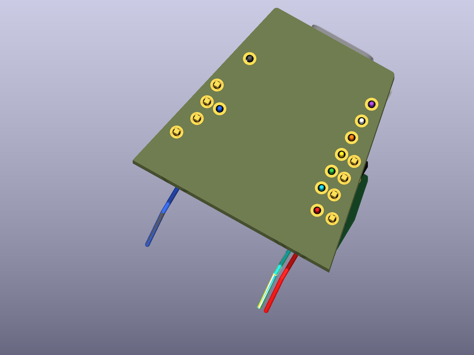
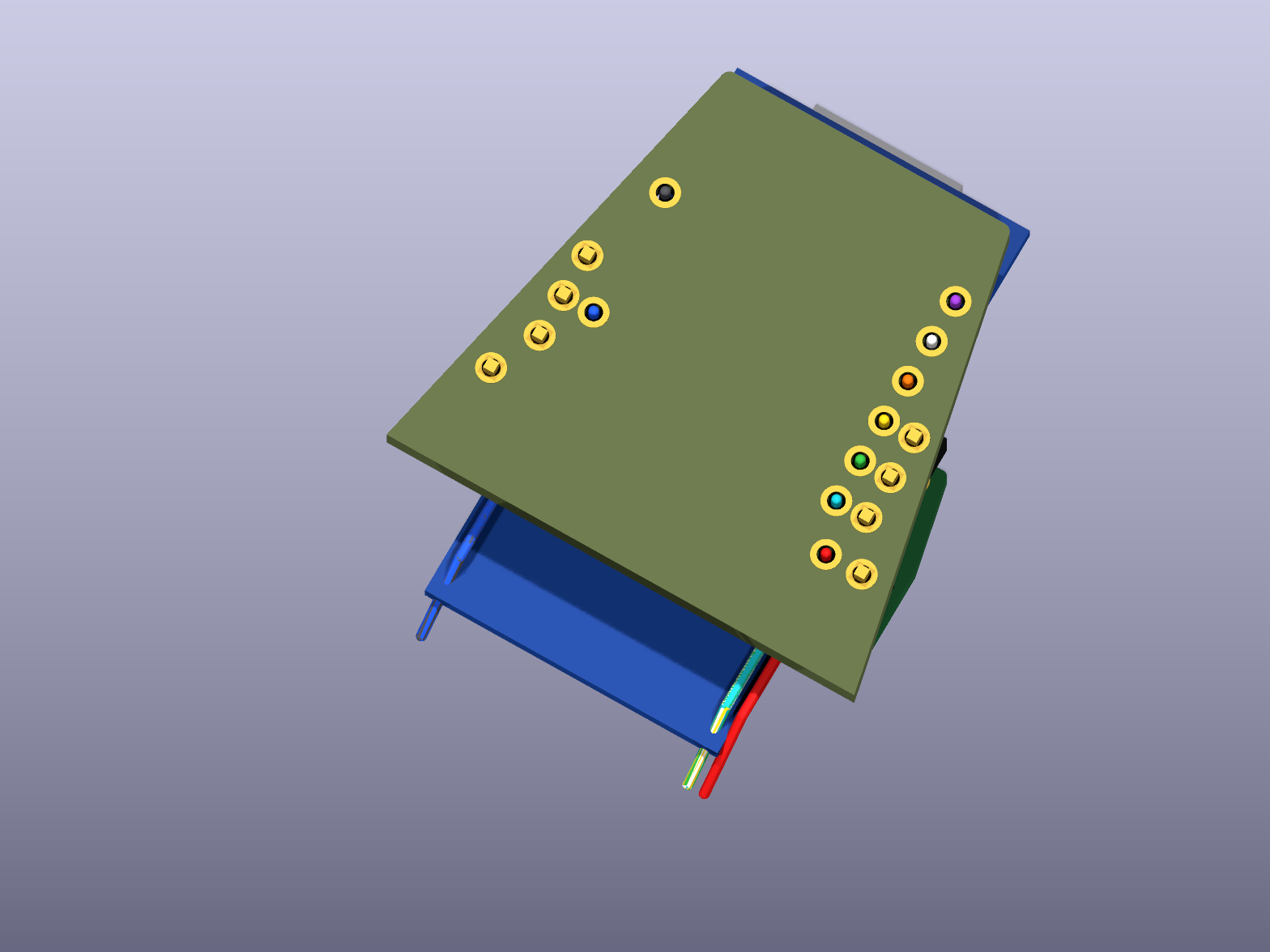
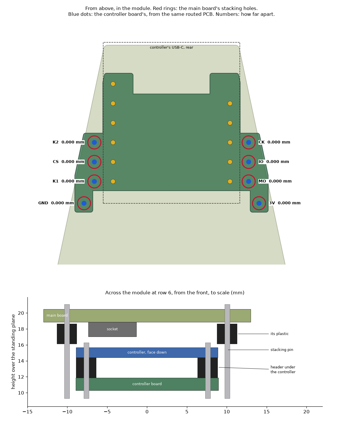
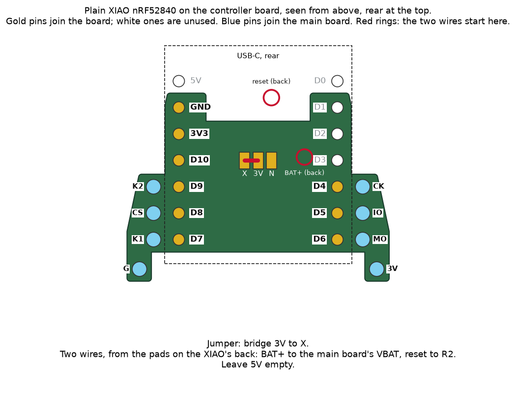
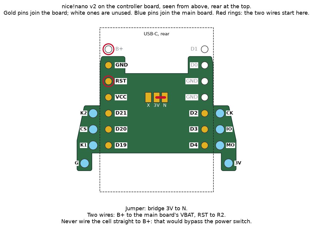
The same breakaway panel holds three boards: main, sensor and controller. Snap them apart and file the stubs. It supports a nice!nano v2 or a plain XIAO nRF52840, with the firmware the only difference: the six signal pins are GPIOs on both. The controller stands face down on a 2.54 mm header on its own small board (two straight columns 15.24 mm apart), and eight stacking pins join that board to the main board above it. One solder jumper picks the 3.3 V pin, and two short wires carry the battery and reset.
On the panel the controller board lies a quarter turn round; in the module it sits under the main board, and each of its eight stacking holes lines up with one of the main board's. Both controllers use the same pin rows. A XIAO's rows sit 0.2 mm further from its USB-C mouth, so its mouth lies 0.2 mm inside the module's back. All images are nominal models, not a physically tested fit for every controller or clone.
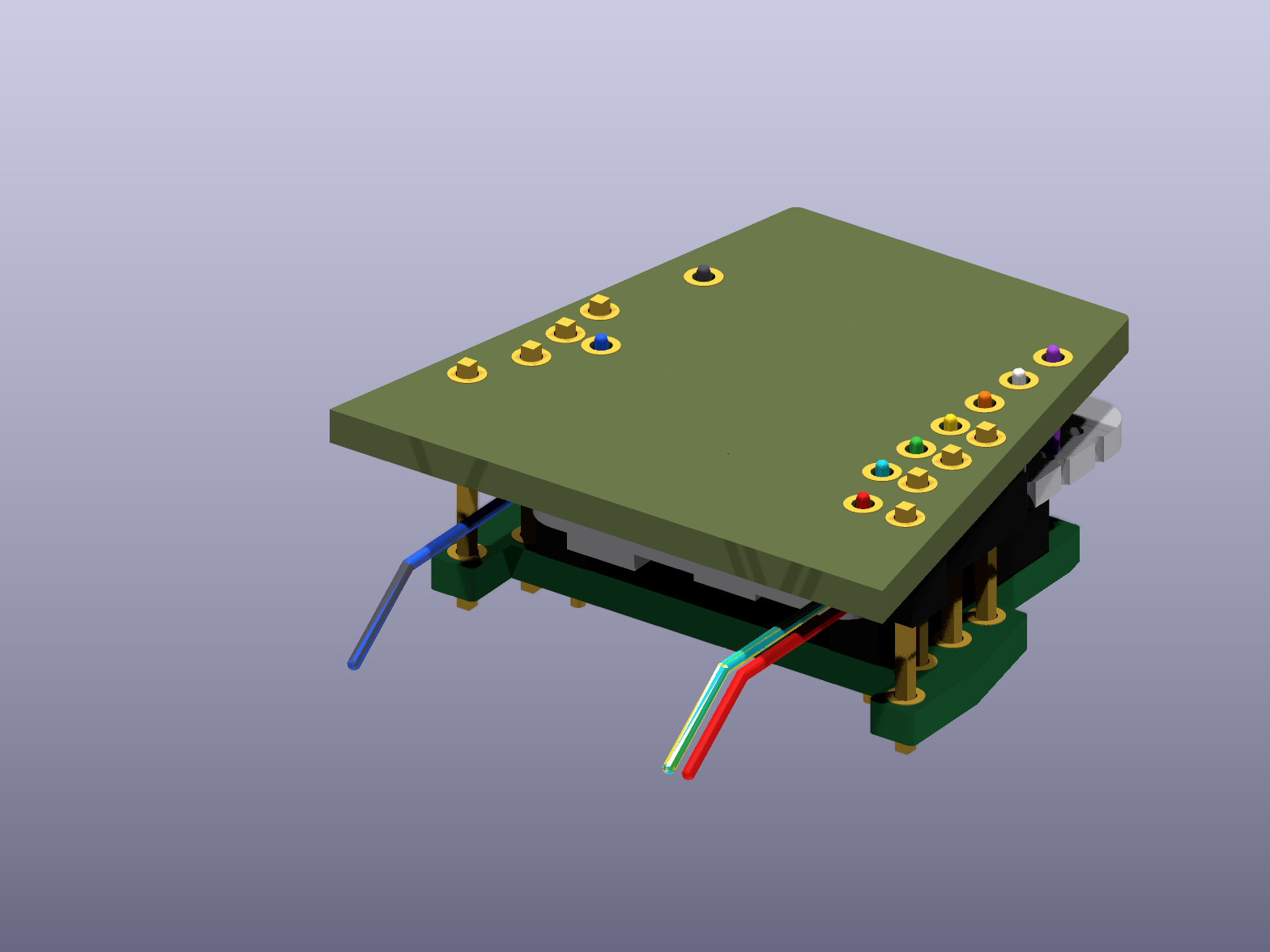
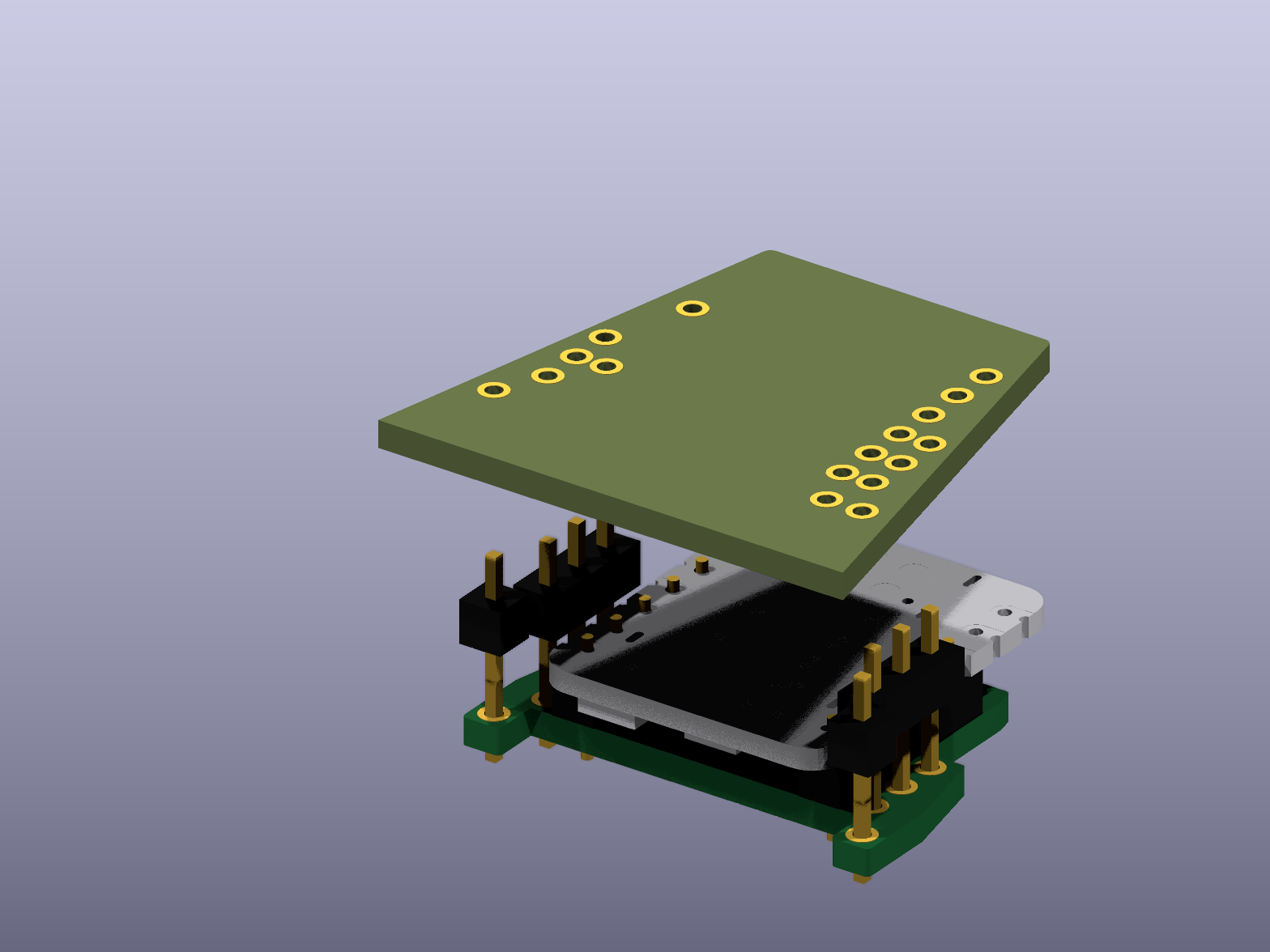
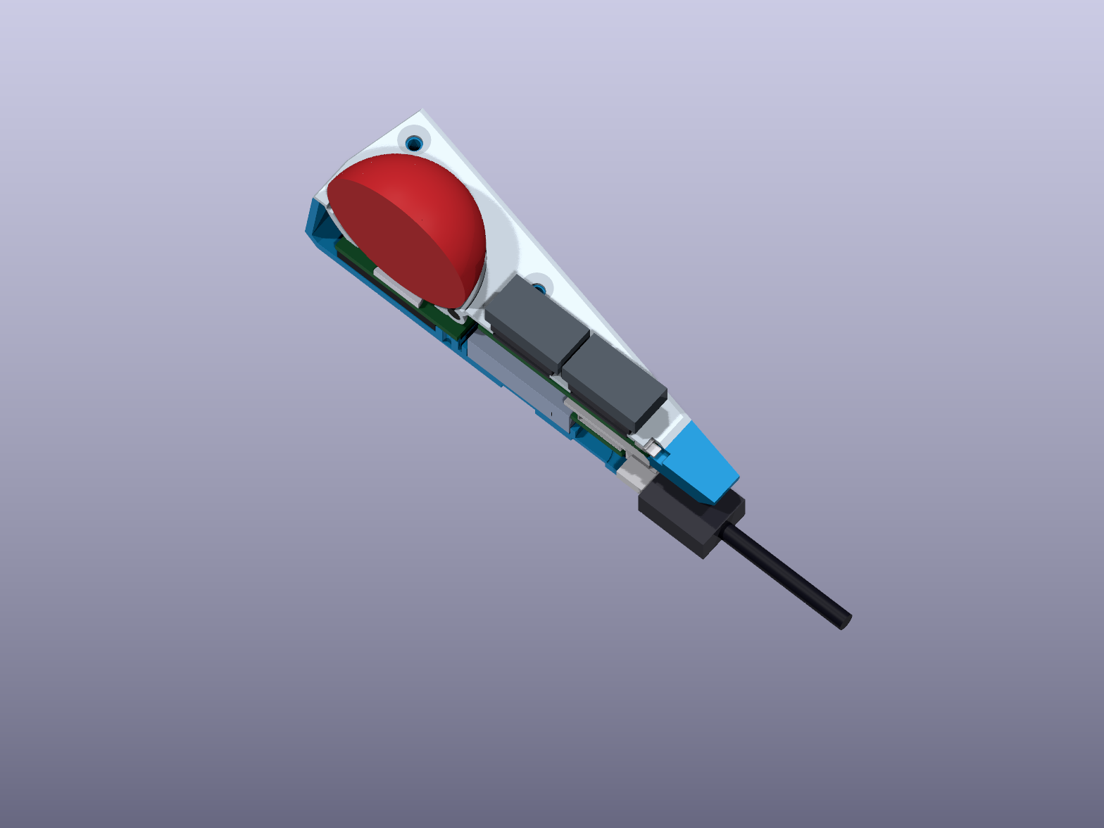
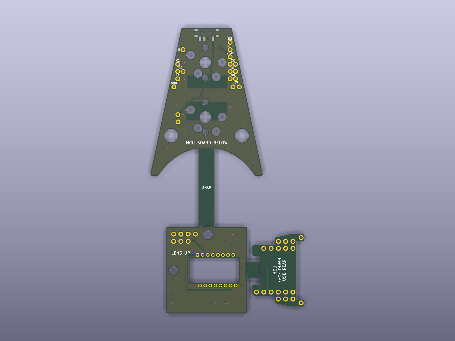
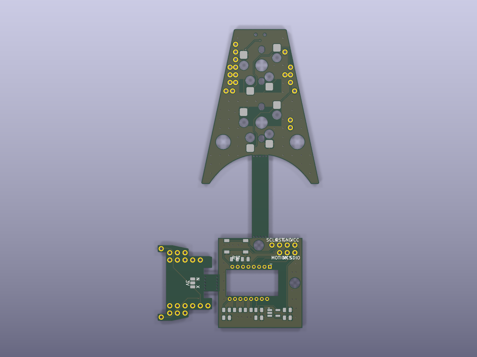
Bill of materials
Quantities are for one keyboard (both halves). The PCB is reversible, so both halves use the same board. "Spares" are worth ordering because AliExpress packs come in round numbers anyway.
| # | Part | Qty | Search AliExpress for | Notes |
|---|---|---|---|---|
| 1 | PCB, fab/prisma_jlcpcb.zip |
2 (order 5) | (JLCPCB, not AliExpress) | 2 layers, 1.6 mm, 87.6 × 92.3 mm, HASL, any colour. The cheapest tier: 5 boards is 2 keyboards plus a spare. |
| 2 | Seeed Studio XIAO nRF52840, or NologoTech Super52840 | 2 | Seeed XIAO nRF52840 / Super52840 or MINI NRF52840 18x21 |
The same board takes either; set its battery selector to match (BUILD.md, step 1). XIAO: the plain one (not "Sense", not "Plus"), genuine Seeed, since the board relies on its bottom pads (BAT, GND, NFC1). Super52840: the one with B+/B- pads and a row of nine GPIO pads underneath. |
| 3 | Kailh Choc v1 switches | 24 (+2) | Kailh choc low profile switch |
Any v1 (PG1350) switch. Not v2 (MX stem) and not Choc mini. |
| 4 | Kailh Choc hot-swap sockets | 24 (+4) | Kailh choc hotswap socket PG1350 |
CPG135001S30, the low-profile socket. |
| 5 | Choc keycaps, 1u | 24 | MBK keycaps choc / CFX choc keycaps |
All 24 are 1u (17.5 × 16.5). Thumbs and pinky too. |
| 6 | LiPo battery, 500 mAh, 3.7 V | 2 | 702040 lipo 500mah JST PH 2.0 |
Nominal 7 × 20 × 40 mm, for the halves only. Verify the seller's actual dimensions, lead exit and protection board; ask for the JST PH 2.0 plug and check polarity. |
| 7 | JST PH 2.0, 2-pin, SMD horizontal socket | 2 (+2) | JST PH 2.0 2P SMD horizontal |
S2B-PH-SM4-TB footprint: side entry, two signal pads and two big mounting tabs. |
| 8 | Slide switch MSK-12C02 | 2 (+3) | MSK-12C02 SMD slide switch |
The 7-pad SMD one with two locating pins. |
| 9 | Reset button: SMD tact switch 5.1 × 5.1 mm, 2.0 mm tall, 4 gull-wing legs (XKB TS-1187A-B-D-B or equivalent) | 2 (+3) | 5.1x5.1x2.0 SMD tactile switch 4 pin |
On the switch face, in the nook above the thumbs: reset, or double-tap for the bootloader, with the case closed. The height matters: 2.0 mm puts the plunger 0.2 mm under the plate's top. The common 1.5 mm one (LCSC C318884) fits too, but then sits 0.7 mm down and needs a fingernail or a pen tip. |
| 10 | Disc magnets 8 × 1.5 mm, N52 | 26 (+4) | 8x1.5mm N52 neodymium magnet |
Thirteen per half: four stacking positions, three circular stand contacts, six inner-wall magnets evenly spread at 17.8 mm pitch. The same part is used in every accessory. |
| 11 | M3 × 8 flat-head screws, 90° countersunk (ISO 10642 / DIN 7991) | 8 | M3x8 countersunk flat head screw |
Four per half: through the plate (the head sits flush in its countersink) and the PCB, threading into the solid base (2.5 mm pilot holes). |
| 12 | Silicone bump-ons 8 × 2 mm, self-adhesive | 10 (+6) | 8x2mm silicone bumpon self adhesive |
Five per half, in the slots under the floor (see BUILD.md). The specified height preserves stacked fit; they lie outside the centred 54 mm stand contact circle. |
| 13 | Filament | ~170 g | Nylon (PA) | Case left + right (solid base, 65.9 cm³ each) and the two top plates (4.3 cm³ each); approximately 160 g solid nylon before print overhead. |
Cyberdeck dock (optional): case/dock.stl (about 83 cm³, 95 g of Nylon), for a Ugreen folding phone
stand with an 85 × 105 × 4 mm base, or on its own as a tented unibody. Print it flat side down, with
supports inside the pocket (its roof spans 85 mm). It takes 31 common 8 × 1.5 mm discs:
12 under the halves (six per half), 12 in the drawer walls (six per side), 6 for the three base-magnet
pairs and one in the drawer floor. The side magnets face all six seam magnets outside; positions 2, 4
and 6 also face the insert through a 0.6 mm inner skin. Load them from outside, flush, then glue in
place. A magnet chain must attract throughout: half → dock → insert. Three base discs go in the dock
and three are glued on the aluminium Ugreen base, paired with opposite poles facing. Add 6 more
8 × 2 mm bump-ons, three under each wing.
Independent tenting (optional): two stands with steel tilting phone platforms. The owner
confirmed magnetic attraction on the actual supports. No extra discs: the existing case
magnets meet the steel directly. Use the mirrored SVGs in case/ for alignment only.
Minimum centred clear flat contact circle 54 mm; prefer about 60 mm if it clears the
feet and obstructions. Attraction alone does not qualify retention at a typing angle.
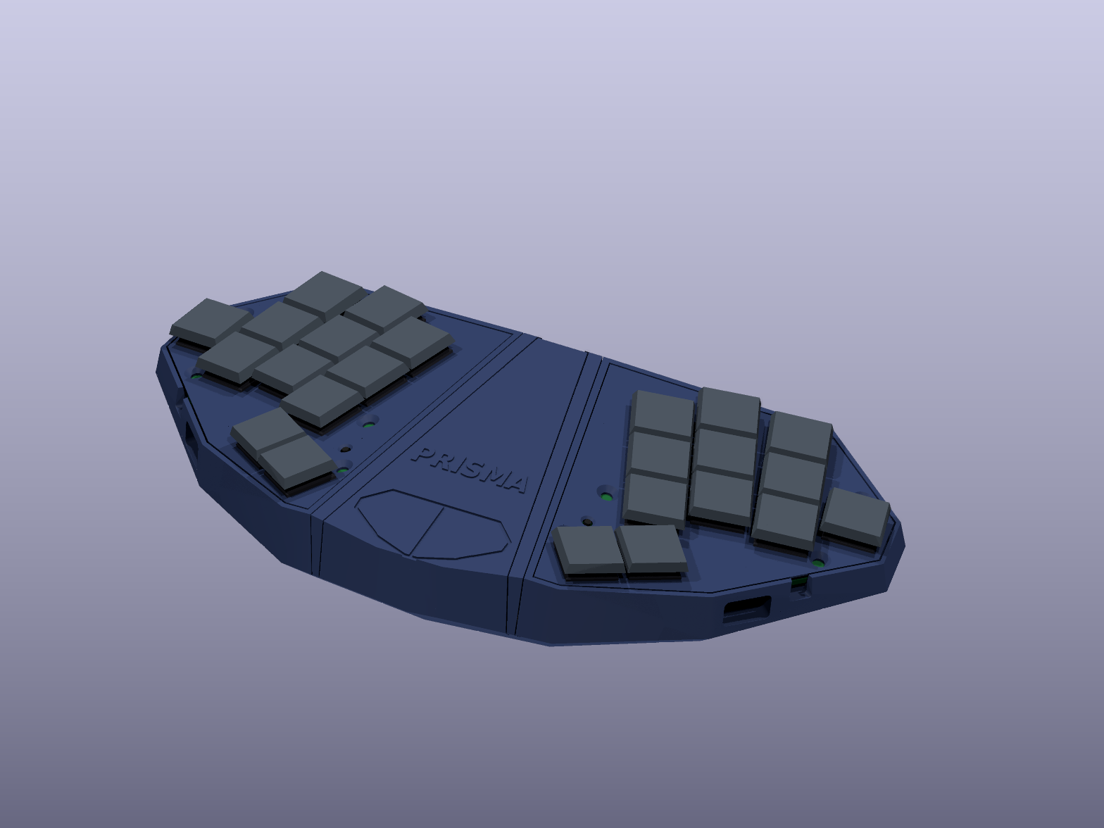
Drawer placeholder: case/insert.stl (71.6 cm³, solid, with PRISMA in low relief), for when neither module is in the drawer:
6 common discs, three a side.
Magnet total: both halves 26 + dock and base 31 + placeholder 6 + both pointing modules 14 = 77 discs, before spares. The three discs glued to the dock stand's aluminium base are unchanged; these are separate from the independent steel platforms.
Drawer modules (optional). Either slides into the dock's drawer from the front, or snaps onto either half's inner wall on the desk. Everything below is per module, and most of it is the same part you already buy for the halves.
| Every module | Qty | Search for | Notes |
|---|---|---|---|
Printed tray, case/module_tray.stl |
1 | The same print for every module | |
| Printed lid | 1 | trackball/case/lid.stl (MX), trackball/case/lid_choc.stl (Choc v1) or trackpad/case/lid.stl |
|
PCB, trackball/fab/trackball_jlcpcb.zip |
1 (order 5) | (JLCPCB) | 2 layers, 1.6 mm, 53.7 × 99.5 mm. One breakaway panel of three boards (main, sensor, controller), for both pointing modules and either controller: nice!nano v2 or plain XIAO nRF52840. JLCPCB may count this as three designs and add a fee: enter Different Design = 3 and confirm on the quote |
| M3 × 8 flat-head screws | 6 | same as item 11 | Four through the lid unchanged; finish the two sensor-board screws to ≤7.6 mm overall, deburr, then verify seating, engagement and ≥0.3 mm tip clearance before installing electronics/battery (BUILD.md) |
| Disc magnets 8 × 1.5 mm, N52 | 7 | same as item 10 | Three a side, one in the floor |
| Silicone bump-ons 8 × 2 mm | 3 | same as item 12 | |
| Slide switch MSK-12C02 | 1 | same as item 8 | On the main board, lever out of the back wall |
| Reset button TS-1187A | 1 | same as item 9 | On the sensor board, facing down |
| nice!nano v2 or clone | 1 | nice!nano v2 / SuperMini nRF52840 |
Face down on the controller board's header, USB-C flush with the back. Only a genuine nice!nano v2's pin rows have been checked: compare a clone's against the wiring diagram before soldering |
| Alternative to nice!nano: plain XIAO nRF52840 or Super52840 | 1 | same as item 2 | Same panel and header; set its jumper and use its own firmware. Its USB-C mouth sits 0.2 mm inside the back. Real fit and operation remain unverified; Super52840 support is experimental |
| Compatible 2.54 mm-pitch pin header | 11 pins | 2.54 mm round pin header 0.6mm |
Two 5-pin lengths and a loose pin, under the controller. Plastic 2.54 mm thick. Measure actual pins and controller holes: standard 0.64 mm square pins interfere with the Ø0.75 mm Seeed reference holes; round Ø0.6 mm is a candidate, not a hardware qualification. Never force pins |
| Extra-long 2.54 mm pin header, 15 mm | 8 pins | 2.54 mm header 15 mm long |
Stacking pins between the controller board and main board: two 3-pin lengths and two single pins. Check where the plastic sits: short end at least 2.35 mm, long end at least 6.7 mm |
| LiPo battery 752025, 250 mAh | 1 | 752025 lipo 250mah |
7.5 × 20 × 25 mm, not the halves' larger cell. Over 20.5 mm wide, it fouls the controller board's arms |
| 30 AWG stranded wire | 80 to 100 mm per wire | 30 AWG silicone wire |
About 25 mm for the two wires from the controller |
| Trackball | Qty | Search for | Notes |
|---|---|---|---|
| PixArt PMW3610DM-SUDU + LM18-LSI lens | 1 + 1 | PMW3610 (eBay, Tindie: Randware) / LM18-LSI |
Through-hole sensor in the sensor board's cut-out, on its back face; the lens clips on from the front, looking up |
| TLV74318PDBVR, SOT-23-5 | 1 | TLV74318PDBVR |
The sensor's 1.8 V |
| 0805 capacitors: 10 µF, 3.3 µF, 1 µF ×2, 100 nF ×3, 10 nF ×2; 0805 resistor 10 kΩ | 9 + 1 | 0805 capacitor kit |
Values as siderakb's PMW3610 board (CERN-OHL-P), which this circuit follows |
| MX switches + Kailh MX sockets + 1u DSA caps, or Choc v1 switches + Choc sockets + caps | 2 each | Kailh MX hotswap socket / item 4 |
Populate only one socket family. Choc v2 is not supported |
| 34 mm trackball, 3 mm Si3N4 balls | 1 + 3 | 34mm trackball / 3mm ceramic ball Si3N4 |
The ceramic balls glue into the cup's three pockets |
| Trackpad | Qty | Search for | Notes |
|---|---|---|---|
| Cirque TM040040-2023-302 or I²C-configured kit | 1 | Cirque 40mm I2C flat overlay |
Use the supplied I²C breakout and flat cable; on SPI-labelled kits remove R1 for I²C, keeping R7/R8 for 3.3 V |
| Supplied I²C breakout with pull-ups + 12-pin FFC | 1 + 1 | supplied with the kit | Reserved maximum breakout envelope 24 × 18 × 4.5 mm; confirm actual size and FFC contact orientation. Four MCU wires to breakout, separate DR wire directly to Cirque underside |
| Choc v1 switches, sockets and keycaps | 2 + 2 + 2 | same as items 3, 4, 5 | Compact caps only: 17.5 × 16.5 mm, rotated with the switches (17.5 mm front-to-back here). Centred nominal pad gap 0.585 mm, potentially 0.285 mm after radial seat play; verify actual placement/travel/wobble. |
Consumables: thin solder (0.5–0.6 mm), flux, a little kapton tape, thin double-sided tape (0.25 mm at most) for the controller board's seats, CA glue or epoxy for the magnets, removable adhesive dots for the trackpad, thin card for the sensor's shims, and a 2.5 mm insulating spacer/tape stack for the I²C breakout (no printed holder).
Soldering, assembly and printing: see BUILD.md.
Soldering and assembly
The module, battery and battery socket all end up inside the case, under the PCB. Only the USB-C port and the power-switch lever show, through openings in the outer wall: a recess the size of a cable's plug in front of the port, and a slot open to the top for the lever. Push the lever with a fingernail. The module's LED and its own reset button face the case floor, so flash and test it before closing the case. A second reset button on the switch face, wired to the module's reset pad, works with the case closed: it sits in a cone in the plate, above the thumbs.
Everything is soldered with an iron: no paste, no hot air. Build one half at a time. Both halves use the same PCB, turned over for the right half.
The module is a Seeed XIAO nRF52840 or a NologoTech Super52840. The board takes either: a battery selector, set in step 1, matches it to your module. The other steps are the same for both.
Tools
- Temperature-controlled iron with a small chisel tip (1.6–2 mm) for the module, sockets and JST tabs, and a fine conical tip for the power switch.
- Leaded solder: about 330 °C.
- Lead-free: about 360 °C.
- Thin solder (0.5–0.6 mm), a flux pen, fine tweezers, kapton tape, isopropyl alcohol and a brush.
- A multimeter with a continuity beep.
- Optional: a magnifier or phone camera to inspect the small pads.
The two faces
Each board has a parts face and a switch face. The silkscreen tells you which is which:
| Half | Parts face (silkscreen) | Switch face |
|---|---|---|
| Left | LEFT: parts on this face |
the other one |
| Right | RIGHT: parts on this face |
the other one |
- Parts face: the module, power switch, JST socket and the 12 hot-swap sockets. It faces the case floor.
- Switch face: the key switches clip in here, the reset button is soldered here, and you bridge the jumpers and fill the module's holes from this side.
The module always lies flat on the parts face, with its pad side against the PCB and its components (USB-C, shield, reset button) pointing away from it, towards the case floor.
Before you start
- Flash and test the module first. Plug it into USB and double-tap reset: a USB drive appears. Copy the firmware onto it:
| Half | With a dongle | Without a dongle |
|---|---|---|
| Left | prisma_peripheral_left-zmk.uf2 |
prisma_central_left-zmk.uf2 |
| Right | prisma_peripheral_right-zmk.uf2 |
prisma_peripheral_right-zmk.uf2 |
A dead module is much easier to swap now than after soldering.
- Battery size and polarity. The halves use nominal 7 × 20 × 40 mm, 500 mAh cells; the trackball and trackpad keep 752025, 250 mAh cells. Verify actual dimensions and lead clearance before assembly. Silkscreen
+marks pin 1 of the JST socket. Cells ship with either polarity: check the plug with the multimeter. If reversed, swap the two crimps in the disconnected plug housing (lift each tab with a needle), keeping the contacts insulated from each other. - Magnet polarity. Every left-half magnet goes in with the same pole facing out, and every right-half magnet with the other pole. That makes both the stack and the side-by-side join attract. Mark one face of each magnet stack before you start.
1. Bridge the D0–D2 jumpers and the battery selector (switch face)
On the switch face, inside the module's outline, there are three small pad pairs labelled D0, D1, D2, on the face without the module. Flux them and bridge each pair with a small blob of solder.
Next to them is the battery selector: two rows of two pad pairs, labelled +MID and +USB. The two modules have their battery pads in the same spots, swapped, and the row you bridge decides which battery hole is +:
| Module | Bridge both pairs in row |
|---|---|
| Seeed XIAO nRF52840 | +MID (its + pad is the one nearer the module's middle) |
| Super52840 | +USB (its B+ pad is the one nearer the USB end) |
Bridge one row only. Both rows short the battery; the wrong row connects it backwards. Both halves get the same row.
Left: the left half's switch face. Right: the right half's switch face. Bridge the three D0–D2 pairs and one selector row, and later fill the three boxed hole groups (step 2).
Leave the jumpers on the other face open: they're on the parts face, under where the module will sit.
Check: each bridged pair beeps on the multimeter, and the unbridged selector row doesn't.
2. Solder the module (parts face)
- Pre-tin the module's underside pads that the boxed holes reach: the two battery pads (VBAT and GND on the XIAO, B+ and B- on the Super52840), the P0.09 pad (NFC1 on the XIAO,
009on the Super52840) and RST. Flux each one and touch it with a lightly tinned iron, leaving a thin, flat coat. Wick off any bump: a blob lifts the module off its edge pads. In step 4 the solder fed into each hole then only has to melt into the coat that's already there. - Flux the 14 edge pads. Lay the module flat over its outline with the USB-C end towards the board edge. The pads are pulled out past the module, so you can reach them from the side.
- Tack two opposite corners: put solder on the iron, touch it to the board pad and the castellation together, and let it flow. Check the module is flat and every castellation sits over its pad. Reheat a corner to adjust it.
- Solder the other 12 edge pads the same way: iron on the board pad, solder fed into the castellation. Each joint should be a small concave fillet up the half-hole.
- Turn the board over (switch face up). Fill the boxed holes: the pair inside one box (the battery), both holes in the second box (P0.09: one under each module's pad, so fill both), and the round hole in the small square box near the USB end (RST, the module's reset pad). Hold the iron on the ring for 2–3 s and feed solder into the hole until it fills and stops sinking. This alone does not prove a good joint: check continuity to accessible points on the module and inspect for shorts before applying power. Fill only the boxed holes. The unboxed ones belong to the other half. Most sit under bare module areas; the unboxed reset hole sits under the module's GND test pad, and only wires to the other half's (empty) button pads, so it does no harm either way.
- Clean off the flux.
The battery holes and one P0.09 hole are smaller than the rest (0.6 mm, as large as the pads above them allow): flux them well, use thin solder (0.5 mm), and hold the iron on the ring until the solder sinks into the hole before you feed more.
Check:
- Before any battery goes in: the power switch's middle pad (VBAT; the switch is fitted in step 3) must not beep to the module's GND castellation. A beep may indicate the wrong selector row, both rows bridged, or another short: find and fix it first.
- The battery hole the selector made + beeps to the power switch's middle pin.
- The RST hole does not beep to GND (the module's reset is pulled up inside the module: a beep means a solder bridge, and the half would sit in reset).
- No two adjacent castellations beep to each other.
3. Power switch, MSK-12C02 (parts face)
It goes next to the module's USB-C, with the lever pointing out over the board edge and its two locating pegs in the small holes.
- Tin one of the four corner (shield) pads. Place the switch with tweezers and reheat that pad to tack it.
- Solder the other three shield pads.
- Solder the three signal pads with the fine tip and very little solder. A bridge between the middle pin and its near neighbour does no harm (both are VBAT). A bridge from the middle pin to the far one bypasses the switch: wick it away.
4. JST battery socket (parts face)
Its opening faces the battery's spot under the inner keys. Tack one signal pin, check it sits flat, and solder the other pin. Then solder the two large mounting tabs: they need more heat and more solder, because they take the force of plugging the battery in.
5. Hot-swap sockets (parts face)
Twelve, one per key. Each socket fits its outline only one way round.
- Tin one pad lightly, place the socket, and hold it flat with tweezers while you reheat the pad until the socket's metal tab sinks into the solder.
- Solder the second tab. Use enough solder to make a fillet, but keep it out of the socket's opening.
6. Reset button, TS-1187A (switch face)
It goes on the switch face, in the gap above the thumb keys, inside its outline labelled RST. The part is square and symmetric: any of the four ways round works.
- Tin one corner pad, hold the button flat and centred with tweezers, and reheat the pad to tack it.
- Solder the other three legs: a small fillet on each, iron on the pad and against the leg. Keep the solder off the body: the button is 2.0 mm tall and the plate's pocket over it leaves only 0.3 mm above the collar.
Check: the RST hole (step 2.4) beeps to the two legs on the RST side of the button (the side with the label), and beeps to GND only while you press the button.
7. Test (before the case)
- Plug in USB. With the firmware flashed and your computer paired or connected, short each socket's two contacts with tweezers. Every key should register.
- Plug in the battery, unplug USB and toggle the power switch: the half should stay connected.
- Press the reset button once: the half reboots (it disconnects and reconnects). Reconnect USB, then press it twice quickly: a USB drive appears (the bootloader), as with the module's own button.
| Symptom | Look at |
|---|---|
| One key dead | That socket's two joints |
| Pinky, ring-bottom or middle-home dead | Its D0–D2 jumper (step 1) |
| Index-top dead (both halves) | The NFC1 / P0.09 hole (step 2.4) |
| Works on USB, not on battery | The battery holes, the selector row (step 1), the power-switch joints, battery polarity |
| Reset button does nothing | The RST hole (step 2.4) and the button's legs (step 6) |
| Half never starts, or keeps rebooting | RST bridged to GND: the RST hole or the button's legs |
| Nothing works | The module's castellations, or the firmware file |
8. Case and plate
The base is solid up to the PCB's underside, with a pocket for every part. The PCB rests on plastic everywhere, which makes the half stiff and quiet. The top plate covers the whole board: the switches clip into it, and a shallow pocket in its underside clears the solder around the module.
- Fit 13 common 8 × 1.5 mm N52 discs per half (polarity!): seven underneath and six along the seam. Dry-fit first, without forcing the plastic, then apply a little suitable adhesive. Keep adhesive off the mating faces.
- Lay the battery in its bay and plug it into the JST socket. The plug and the slack of its leads sit in the bay, between the battery and the socket.
- Lower the PCB, parts face down, into the base. Each part drops into its pocket, the switch lever slides down its slot, and the USB-C port lines up with its recess. Nothing should need force: every pocket has 0.6 mm of clearance, and the PCB 0.5 mm to the outer walls.
- Lay the plate on top, its pillars and screw bosses resting on the PCB, and fit the four M3 × 8 flat-head screws through the plate and PCB. They cut their own thread in the Nylon: turn them in slowly, and stop when the heads sit flush in their countersinks.
- Clip the switches through the plate into the sockets, then fit the keycaps. The reset button now sits under a cone in the plate, between the index finger's bottom key and the thumbs. Its plunger is 0.2 mm under the plate's top, so keycaps and palms don't reach it.
- Anti-slip pads. Each floor has five slots, each long enough for two pads. Stick one 8 × 2 mm bump-on into one end of every slot and leave the other end empty: when the halves are stacked back to back, the other half's pad drops into that empty end, so the floors and magnets still meet.
The rule is the same on both halves: turn the half over and go clockwise round the floor. In every slot, the pad goes in the end you reach second. Then each half's five pads sit in the ends the other half leaves empty.
Clean the slots with isopropyl alcohol first and press each pad down firmly against the slot's roof, centred in its round end. Stack the halves to check: they should close flat, with no rocking.
Optional stands and drawer retention
- Use the same 8 × 1.5 mm N52 discs everywhere. The dock takes six wing magnets and six side magnets per half, three base pairs (three of those discs are glued to the Ugreen base) and one upward-facing disc in the drawer floor: 31 discs total. No underside contact sits near the drawer retention magnet: at least 1 mm of plastic separates their pockets, even with each 0.2 mm off. Leave the rear free for USB and the cable.
- Each drawer insert takes three evenly spaced side magnets per side (seam positions 2, 4 and 6). The halves and dock have six per side at 17.8 mm pitch; the inserts use every other position. Check the full half → dock → insert polarity chain before gluing.
- Each pointing module also takes one disc in its floor, on the centreline, directly above the drawer's. Glue both flush or slightly recessed, opposite poles facing. They grip the module from below, whatever the side magnets manage through the walls.
- The nominal magnet pockets are Ø8.3 mm for 8 mm discs; never force a magnet in.
- To take a module out, hold the dock and push the tip of the rear hood forwards with a finger through the dock's rear passage, then pull the module out of the front. Unplug USB first.
- The USB-C port is nominally flush with the module's back, with nothing under it. Feed a plug through the dock's 12.8 mm rear passage. A 12.35 × 6.5 mm overmold is the nominal modelled envelope, not a guaranteed fit for every plug or printed dock; check the real plug, cable and passage.
- The rear hood and the dock meet at a 45° slope with 0.4 mm clearance.
- For independent tenting, use the tested steel tilting phone platforms. Do not glue extra discs onto them: the half's existing three stand magnets attract the steel directly. The SVG templates in
case/are 1:1 alignment guides; print at 100% and check the 54 mm boundary with a ruler. - The minimum centred contact circle is 54 mm (44 mm magnet-centre circle). All foot positions lie at least 11.55 mm outside its edge, so the feet do not space the magnets off this steel patch. Prefer about 60 mm for more edge margin, checking the actual shape against feet, rubber and lips. Keep magnet faces flush and clean; any recess, coating or adhesive can reduce grip. Use 2.0 mm bump-ons for stacked fit. Start flat, support the half while increasing the tilt, and test slip, peel, typing loads and stand stability before relying on it. The confirmed attraction is not a retention qualification.
Pointing modules
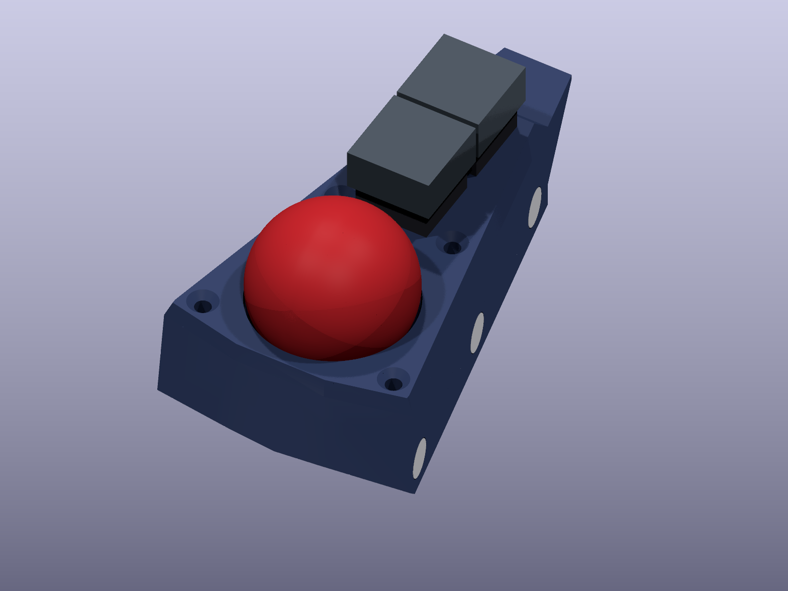
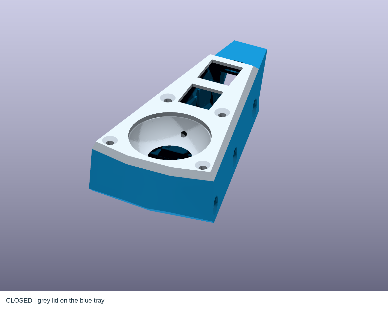
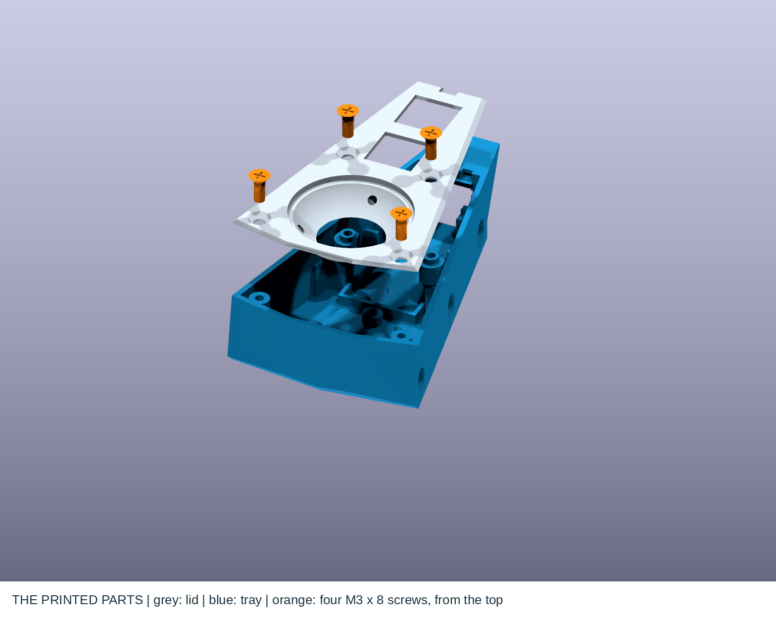
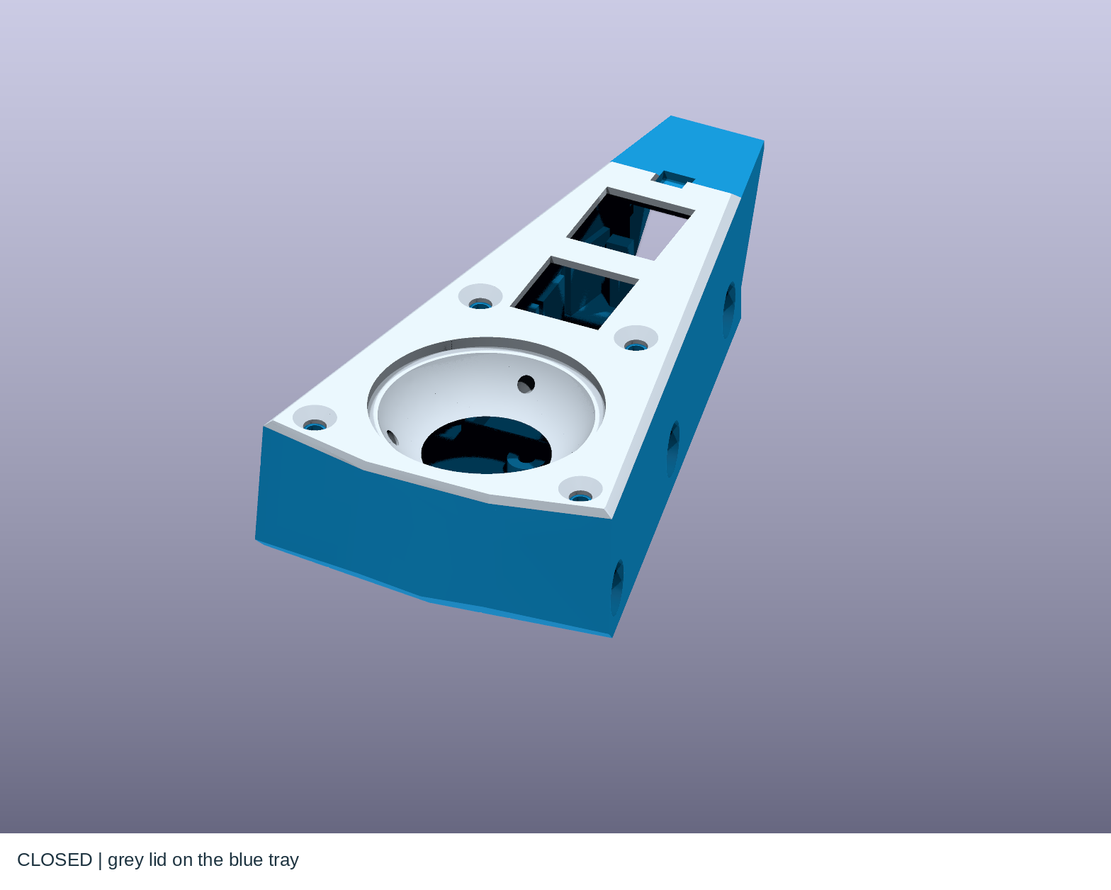
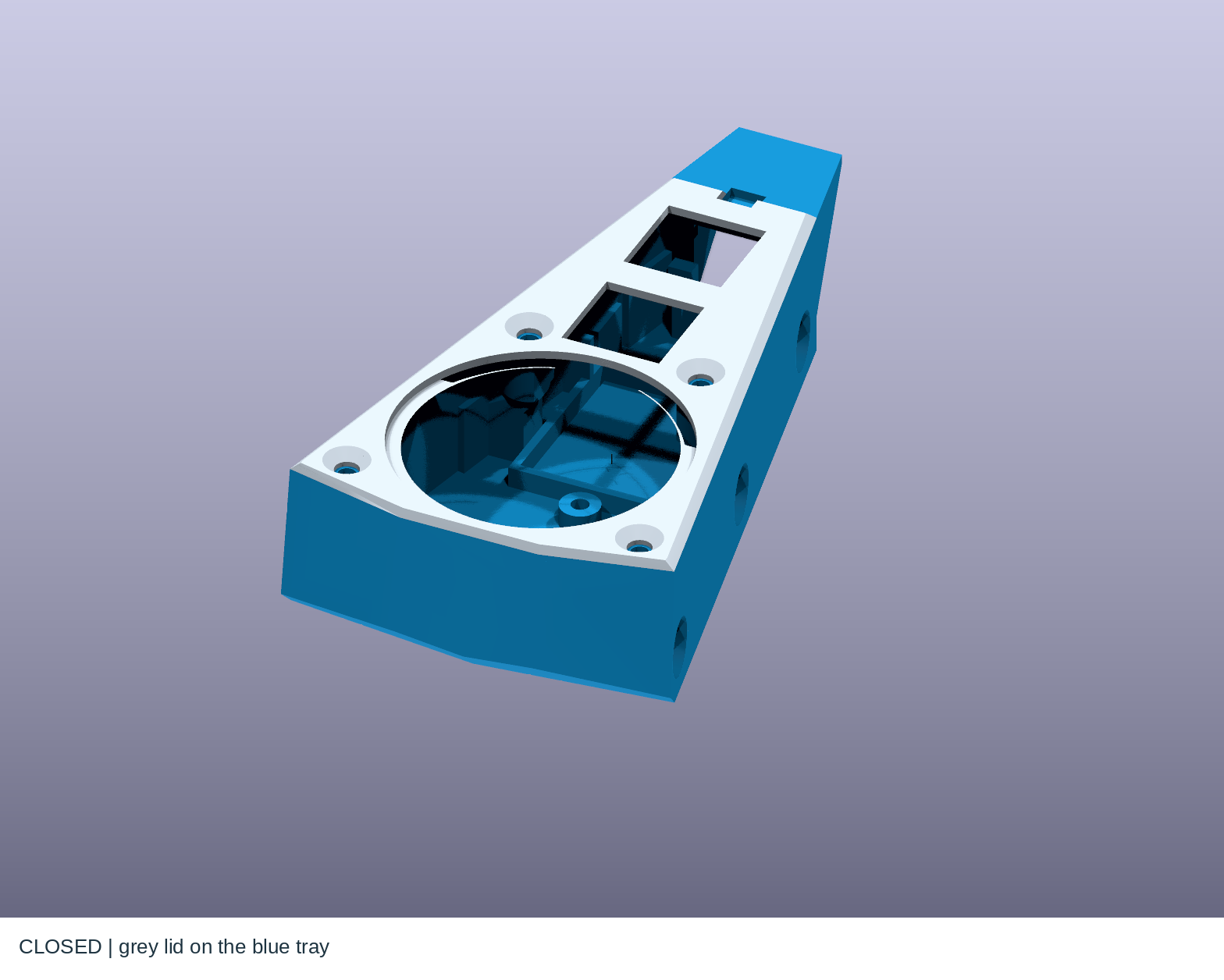
Both modules are built the same way as a half: a tray, a lid, and the same M3 × 8 flat-head screws going in from the top. The tray is one print, shared by all of them. Only the lid changes: trackball/case/lid.stl (MX), trackball/case/lid_choc.stl (Choc v1) or trackpad/case/lid.stl.
The raised lid has upper facets on its front and both sides, starting at the halves' top-surface height. Below that height the front keeps the drawer's matching profile for horizontal removal.
| The parts, lid raised | Closed |
|---|---|
|
 |
 |
 |
|
 |
The same main board holds the two keys and the power switch on both modules. A battery and the controller, on its own small board, sit under it. The same sensor board holds the reset button at the front; on the trackpad it carries nothing else. Everything is hand-soldered with an iron: no paste or hot air. The trackpad retains its supplied I²C breakout and flat cable, plus a separate DR wire.
One panel, either controller: order trackball/fab/trackball_jlcpcb.zip for a nice!nano v2 or a plain Seeed XIAO nRF52840, for either pointing module. The panel has three boards: the main board, the sensor board and the controller board.
The controller stands face down on the controller board on an ordinary 2.54 mm pin header, its pins in two straight columns 15.24 mm apart. Eight stacking pins then join the controller board to the main board above it, beside the controller. The six signal pins land on GPIOs on both controllers, so they need only the right firmware. One solder jumper chooses the 3.3 V pin. Two wires of about 25 mm, the same on both controllers, carry the battery and reset.
The main board does not lift out afterwards: removing it means desoldering the eight stacking pins. Solder and test everything beneath it first.
USB always plugs directly into the chosen MCU's onboard USB-C receptacle. There is no external USB connector, extension or soldered USB wiring.
Boards
- Snap the panel. The main board and sensor board are joined by one long bridge with a row of holes at each end, and the controller board hangs off the sensor board's side, a quarter turn round, on a short tab with a row of holes at each end of its own. The tab meets it in its USB notch. Snap the controller board's tab first, then the bridge: hold a board in one hand and the bridge in the other (pliers help) and bend at the row of holes until it snaps. File off the stubs.
- Main board. Solder the MSK-12C02 power switch on the front face (the side marked
MCU BOARD BELOW), with its lever over the rear edge. Solder one family of hot-swap sockets on the back face: Kailh MX for the MX lid, Choc for the Choc lid and the trackpad. Never both. - Sensor board, trackball. Solder the regulator, capacitors, resistor and TS-1187A reset button on the back face, the PMW3610 in its cut-out, and clip on the lens.
-
Sensor board, trackpad. Solder only the TS-1187A reset button, on the back face.
-
Controller board.
- Set the jumper, on the underside, the face without
MCU FACE DOWN. Bridge the middle3Vpad toXfor a XIAO orNfor a nice!nano. Never bridge all three: on a nice!nano that ties reset to the 3.3 V rail.- Fit a compatible header. Measure the actual controller's holes and the pins before soldering. The Seeed reference has Ø0.75 mm holes: a common 0.64 mm square pin has a 0.905 mm diagonal and does not fit that model. Do not force it or enlarge plated controller holes. A 2.54 mm-pitch header with round Ø0.6 mm pins is a candidate, not a confirmed fit; verify pin diameter, actual hole tolerance, plastic height (2.54 mm) and solder engagement. The reference came from Seeed's Sense resources, so confirm the selected plain XIAO or clone separately. Cut two compatible 5-pin lengths. Set the short ends down through rows 3 to 7 of each column from the top face, so the plastic sits on the top face and the long ends stand up, then solder them from underneath. Pull one compatible loose pin from a spare length and solder it into the left column's row 2, the single hole behind the strip, at the USB end, at the same height: the tray's magnet boss leaves no room for plastic there. Trim the tails underneath to about 1 mm.
- Flash the controller first, while its reset is in reach, then fit it face down, its USB-C over the notch. Rest it on the plastic, level, and solder the pins on its back. Trim them to 0.6 mm at most above the controller: the sockets are close above it. Power it from USB and check that it connects: its keys and sensor are not joined until the stacking pins are soldered. Solder its two wires now, about 25 mm each: battery and reset, from the table under Wiring. They will not reach the main board yet.
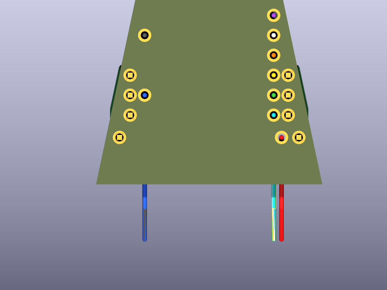
- Fit the stacking pins last, keeping them square. Use 15 mm extra-long header with a short end of at least 2.35 mm and a long end of at least 6.7 mm: two 3-pin lengths for the columns beside the controller, and one pin each for the two outer holes. Sand the cut ends of the plastic flush, so they sit square. Their plastic belongs near the main board's underside, not this board. Fit the short ends up into the main board's eight stacking holes. On the left, three in a line:
K2, the outer hole of the joinedCSpair, andK1, withGNDset further out ahead of them. On the right, the outer holes of the joinedCK,IOandMOpairs in a line, and the outer hole of the joined3Vpair set further out ahead of them. The stackingGNDis not the pad markedG, which takes a wire. Then stand the main board over this board on a 6.75 mm spacer (6.6 to 6.9 mm works), with the long ends down through this board's holes. Solder them to this board only, from underneath. Lift the main board off, and trim the tails underneath to about 1 mm.
How the stacking pins meet the main board, in the module: on the panel the controller board lies a quarter turn round, but each of its eight stacking holes sits exactly under one of the main board's. The diagram is measured from the routed board.
| The main board lifted off the stacking pins | Assembled, seen from above | |
|---|---|---|
| Plain XIAO nRF52840 | |
 |
| nice!nano v2 | |
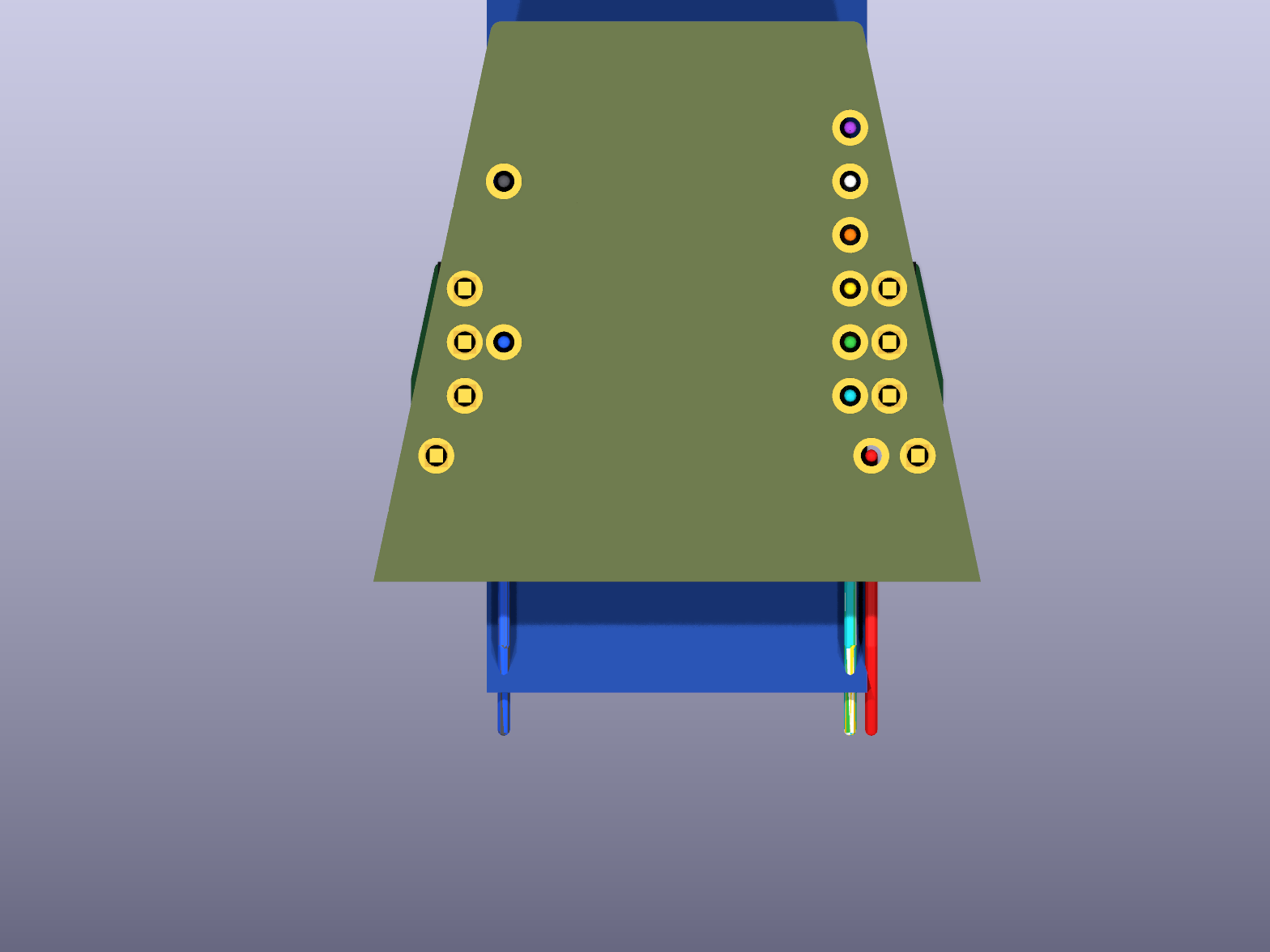 |
Every other hole in the main board takes a wire. Wires: 3V red, G grey, RST white, CK yellow, IO green, CS blue, MO cyan, run forward to the sensor board or trackpad; VBAT orange and R2 purple come up from the controller.
| Plain XIAO nRF52840 | nice!nano v2 |
|---|---|
|
|
For the trackball sensor board, use these values at the PCB references: C1 3.3 µF; C2, C3 and C4 100 nF; C5 and C7 10 nF; C6 10 µF; C8 and C9 1 µF; R1 10 kΩ. Match the regulator and PMW3610 pin 1 to the footprint markings and check the manufacturer drawings before soldering. Solder with an iron, inspect the joints under magnification and check adjacent pins for shorts. Keep the lens clean and do not touch its optical surfaces.
Some sensor-board silkscreen labels overlap. Do not identify wires by silkscreen alone: in the KiCad panel, inspect pad references SJ1 through SJ7, whose nets are respectively S_VCC, S_GND, S_RST, S_SCLK, S_SDIO, S_NCS, S_MOTION. Meter each pad to its intended component or reset button before soldering.
Wiring
Use flexible 30 AWG stranded wire. The main board's pads have short labels: 3V is VCC, G is GND, CK SCLK, IO SDIO, CS NCS and MO MOTION. Solder both of these to the main board before it goes in, and keep it beside the tray on its wires while you fit the parts below it. Run the CK, IO, MO and CS wires inboard of the stacking pins' plastic: that is the only way out of those holes, and a wire left outboard gets trapped. The main board's labels are small: down its right edge, rear to front, the pads are R2, RST, VBAT, CK, IO, MO and 3V, and on its left G and CS, with K2, K1 and GND marking stacking holes.
| From | To |
|---|---|
| Battery + / − | Main board + / - pads (the switch is on the board) |
Sensor board VCC, GND, RST |
Main board 3V, G, RST |
Two wires of about 25 mm run from the controller to the main board, the same on both controllers. Check that length against your own route before cutting. They go on the controller first, and into the main board last, from above:
| Controller | To main board VBAT |
To main board R2 |
Jumper |
|---|---|---|---|
| nice!nano v2 | B+ | RST, on its pin | 3V to N |
| Plain XIAO nRF52840 | BAT+ pad on its back | Reset pad on its back | 3V to X |
Do not connect VBAT to 3V3/VCC, and leave a XIAO's 5V pin empty. The header's row 1 does not reach the board at all, so the battery cannot land on that pin by accident. The same D-number means different GPIOs on these controllers: follow the names in the diagrams and confirm the actual module's markings before soldering.
| Plain XIAO nRF52840 | nice!nano v2 |
|---|---|
|
|
Each signal takes the same controller pin on both modules. The stacking pins carry them, along with G, 3V, K1 and K2:
| Pad | nice!nano v2 pin | Plain XIAO pin |
|---|---|---|
CK |
D2 (P0.17) | D4 (P0.04) |
IO |
D3 (P0.20) | D5 (P0.05) |
CS |
D20 (P0.29) | D8 (P1.13) |
MO |
D4 (P0.22) | D6 (P1.11) |
K1 |
D19 (P0.02) | D7 (P1.12) |
K2 |
D21 (P0.31) | D9 (P1.14) |
On the trackball, also wire the sensor board's SCLK, SDIO, NCS and MOTION to the main board's CK, IO, CS and MO pads, which sit beside their stacking pins.
Verify the clone's pin labels and USB location against a genuine nice!nano v2 before wiring; clones can differ. The power switch is between the cell positive and B+, not between the controller and its regulated VCC. Insulate the battery leads while wiring, check polarity and continuity with the battery disconnected, and confirm there is no short between supply and ground before connecting it.
Use prisma_trackball for nice!nano or prisma_trackball_xiao for XIAO. The XIAO shield turns off I²C1 and the serial port, so that the sensor can use D4 and D5 and the other signals D6 and D7.
On the trackpad, retain the supplied I²C breakout PCB and its 12-pin flat cable. Solder four flexible wires from the breakout's VDD/VCC, GND, SDA and SCL pads to the main board's 3V, G, IO and CK pads. Solder one additional wire directly from the Cirque's underside DR/data-ready test pad to the MO pad; this does not replace the flat cable. Confirm DR by continuity to connector J1 pin 4 before soldering. Use the breakout's two pull-ups to 3.3 V, not 5 V; verify their population and the kit's pad order with its schematic/meter rather than wire colours. Cable orientation matters: check the supplied FFC contact orientation and the breakout's pin reversal before applying power.
Configure the Cirque for I²C: order a TM040040-2023-302 flat-overlay I²C version, or verify the kit's SPI-labelled board has R1 removed. If R1 is still fitted, remove it with a short iron touch and wick away any bridge; protect the nearby FFC connector. Keep R7 and R8 fitted for this 3.3 V design—do not apply the 5 V conversion. See the adapter guide and the Cirque data sheet. Leave the common sensor PCB's trackball components and CK/IO/CS/MO connections unpopulated; wire only its reset and ground (its unpopulated VCC connection is optional).
The firmware uses Zephyr's Pinnacle driver and assumes a directly wired, active-high DR signal. Test startup, motion, primary tap, sleep and wake on the actual pad; interrupt startup and driver calibration have not been physically verified. The PMW3610 trackball firmware likewise compiles but the shared SDIO line and bus turnaround have not been electrically tested.
| Trackpad signal | nice!nano v2 pin | Plain XIAO pin |
|---|---|---|
SCL (breakout), on pad CK |
D2 (P0.17) | D4 (P0.04) |
SDA (breakout), on pad IO |
D3 (P0.20) | D5 (P0.05) |
DR (Cirque underside), on pad MO |
D4 (P0.22) | D6 (P1.11) |
| K1 | D19 (P0.02) | D7 (P1.12) |
| K2 | D21 (P0.31) | D9 (P1.14) |
Breakout GND, on pad G |
GND | GND |
Breakout VDD/VCC, on pad 3V |
VCC (3.3 V) | 3V3 |
Use prisma_trackpad for nice!nano or prisma_trackpad_xiao for XIAO. Both use I²C at 100 kHz and address 0x2A. Never connect breakout VDD/VCC to raw battery voltage or USB 5 V. Both I²C firmware variants compile; physical communications, tap, sleep and wake still need testing.
On the plain XIAO nRF52840, the VBAT and R2 wires start on the two small pads on its back. Keep them flat across its back, not crossing, and off towards the rear of the sockets above it. The battery's negative needs no wire to the XIAO: the - pad is ground on the main board, and ground reaches the XIAO through the stacking pins and header. Use Seeed's front and back pinout to identify the pads on the actual board. Insulate each joint and check polarity and shorts with the cell and USB disconnected.
Super52840: battery-pad locations differ and reset, charger and regulator details depend on the actual revision; compatibility remains experimental until verified against that board's schematic and measurements. Do not assume the Seeed battery, reset or charging pinout applies. The XIAO firmware variants compile but have not been tested on hardware.
Into the tray
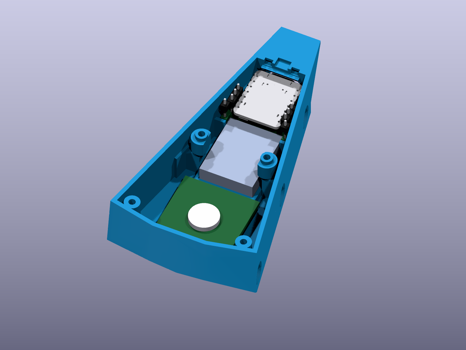
Work in this order, power off, with the magnets already glued in. Before putting the battery in, perform the sensor screw depth check in step 2. The picture shows the first three steps done.
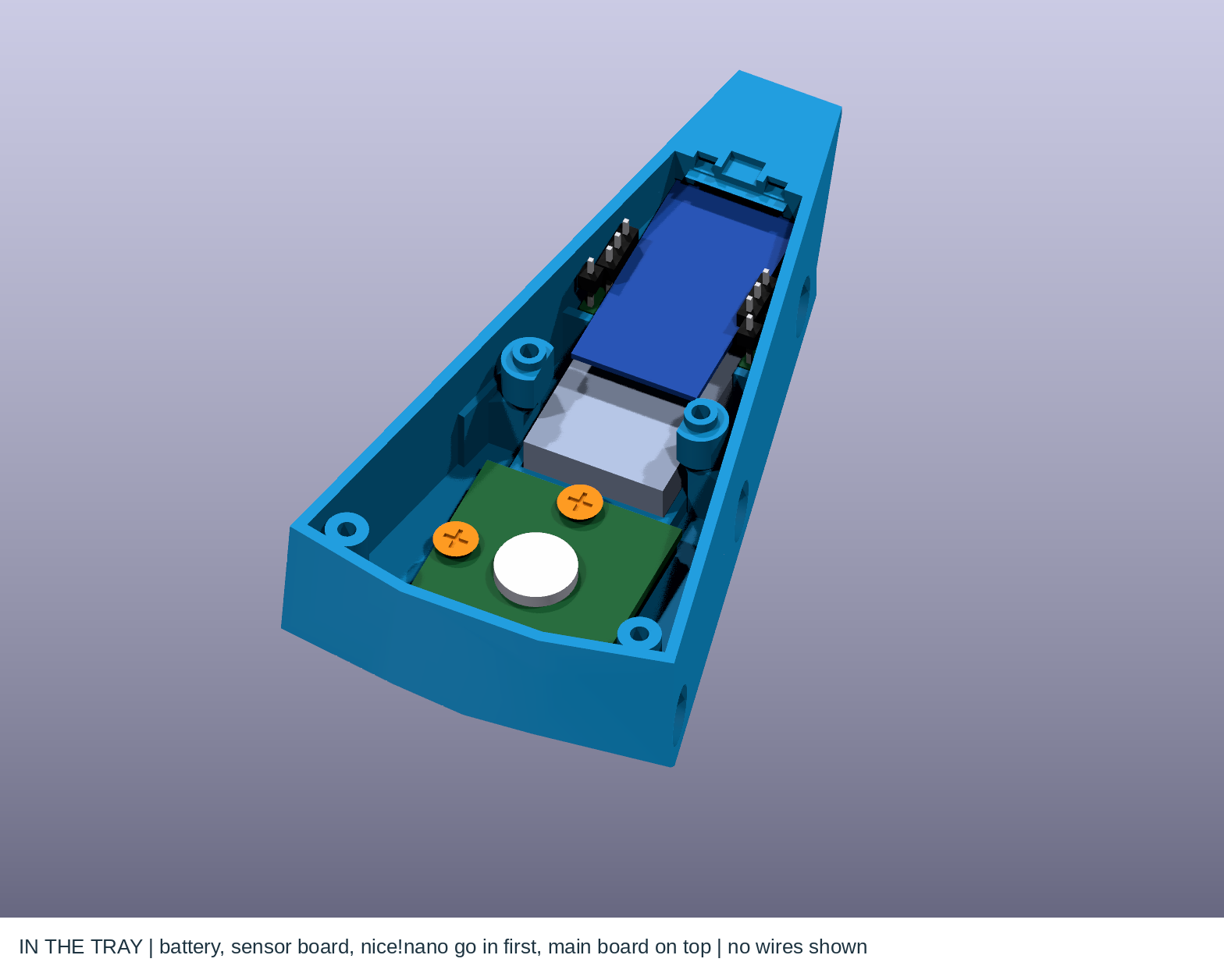
- Battery. Lower it straight into its cradle. Its 7.5 mm thickness has room to spare, but measure a protected pack first, including tape, tabs and leads. Never force it.
- Sensor board. Prepare its two M3 × 8 flat-head screws outside the assembly, before installing electronics or the battery: shorten/file their tips to 7.6 mm maximum finished overall length, deburr and remove all swarf. These are the only screws to shorten. The straight Ø3.4 mm PCB holes are not countersunk: the model's head descends 0.22 mm before seating. An unmodified 8 mm screw bottoms 0.22 mm past the pilot end without a shim; a 0.4 mm shim leaves only 0.18 mm nominal tip clearance. Finished 7.6 mm screws with that shim leave 0.58 mm nominal clearance (0.38 mm with a further 0.2 mm axial uncertainty). Measure the actual head seating, screw length, PCB, posts and shim: retain at least 0.3 mm tip-to-pilot-bottom clearance and sufficient thread engagement. If needed, select a shorter compatible screw or finish it further; never use tightening force to obtain clearance. Trackball: determine the actual unshimmed distance H from the top of the board on the posts to the ball surface on the optical axis with the lid, bearings and ball seated. Measure X from the board top to the lens reference plane specified by the PMW3610 data sheet. Place one equal-thickness shim under each post, each of thickness H − X − 2.4 mm, and verify the assembled reference-plane-to-ball gap is 2.2–2.6 mm. The nominal model gives H = 4.8 mm, but actual dimensions may differ. If the calculated thickness is negative, shimming cannot correct it: do not force the assembly. Do not change optical shims merely to make a screw fit; recheck/shorten the screw for the measured optical stack. Trackpad: no optical gap to set, but put the same 0.4 mm washer under each post because the posts print 0.4 mm low. Fit the board parts face down only after checking screw depth. Actual fastener tolerances and assembled engagement still require physical verification.
- Controller on its board. Hold the stack with the front tilted up, about 18°, and lower it in about 3 mm forward of its place. Move it back so the USB end goes in first: a nice!nano's board edges go into the two pockets in the back wall. Lower the front until the board's ears rest on their seats, with the ribs ahead of its arms and the small posts behind its rear corners. These stops take a plug's push and pull, with about 0.4 mm of play on a nice!nano and 0.65 mm on a XIAO. A thin double-sided tape (0.25 mm at most) on the seats keeps the board down. Check that the USB-C mouth lines up with the opening, and test a real plug before going on. A XIAO's mouth sits 0.2 mm inside the back. The cell's end is 0.4 mm ahead of the board, so make sure no battery tape or wire is caught there.
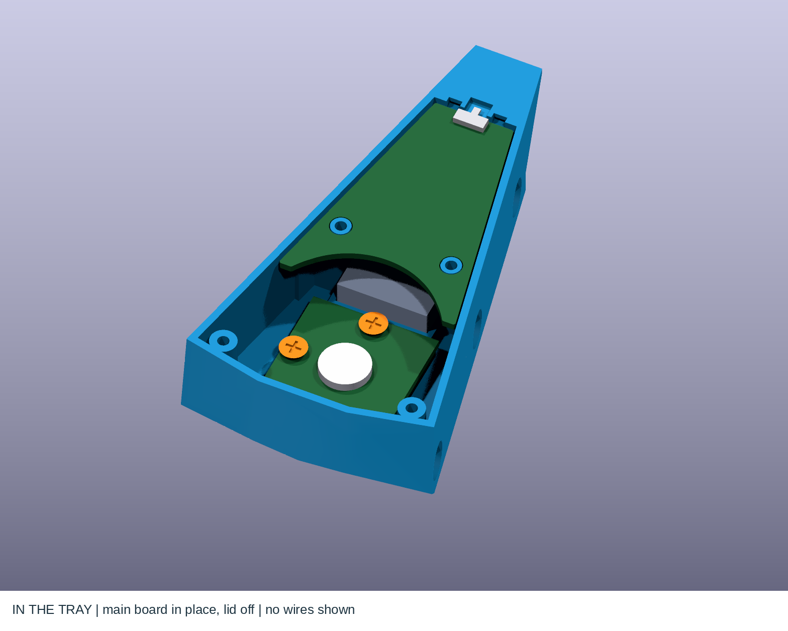
- Main board. Before lowering it, meter the stack:
3Vand ground must not beep together, and each stacking pin must beep to its header pin. Then lower the board flat, feeding the eight stacking pins through those eight holes, and the controller's two wires up throughVBATandR2. The pins' plastic stops about 0.25 mm short of its underside. The two side posts come up through its large holes and it rests on their shoulders and on the ledge at the back wall. The power lever goes down its slot. Solder the eight pins and the two wires from above. Each pin's pad is joined to a wire pad, so its joint may melt that wire's: keep them brief, and keep the joints concave. Trim the pins to 0.6 mm at most: the Choc and trackpad lids sit 1 mm over them, and the lid's lip passes close to the two rear pins, so dry-fit the lid. Now test everything together, before the lid: the battery, the power switch, both keys, the sensor or trackpad, and reset.
- Trackpad only. Confirm the actual pad has a clear support ring and fit it in the lid on removable adhesive dots. Reserve the packing space above the mostly empty sensor/reset board for the supplied breakout: 24 × 18 × 4.5 mm maximum overall, including connector, resistors and solder joints, on a 2.5 mm insulating spacer above the sensor PCB so it clears the screw heads. No printed holder is required. Insulate the breakout's underside and prevent it from moving into screw heads or bare conductors. Keep the original flat cable in its reserved 7 mm-wide bend corridor above the breakout, with slack to lift the lid; route the separate DR lead beside it, and the four breakout wires to the main board's pads. These are explicit clearance envelopes, not measurements of your kit: check its board size, cable length, bend radius and joint height before assembly. Do not sharply fold the FFC or trap it under the lid. Check the complete wired closure before securing the lid.
- Trackball only. Glue the three ceramic balls into the lid's cup.
- Lid. Rear first: tilt the lid, push its two rear hooks into the slots in the back wall, then lower the front. It locates on the tray's rim.
- Four M3 × 8 screws into the lid's countersinks, as on a half: they go into the tray's four posts. Turn them in slowly, and stop when the heads sit flush.
- Clip the switches through the lid into the sockets, fit the keycaps, and drop the ball in. On the trackpad, use 17.5 × 16.5 mm compact Choc caps. Conventional twin-stem caps rotate with the switch, putting 17.5 mm front-to-back here; do not assume they can turn independently. The centred nominal pad gap is 0.585 mm; an 18 mm square envelope has only 0.335 mm. The seat's 0.3 mm radial play can reduce those gaps to 0.285/0.035 mm before other tolerances. Centre and secure the pad with the actual adhesive, then verify full key travel and wobble without contact. Stop if tolerances cannot preserve clearance; nominal tests do not guarantee fit. Use the current tray and lid together: the front screw pair moved 1.5 mm outwards to retain a 2.087 mm screw-to-pad-seat web. Tighten only to flush, never to force a distorted lid flat.
Stick three 8 × 2 mm bump-ons into the floor's recesses.
Power and reset
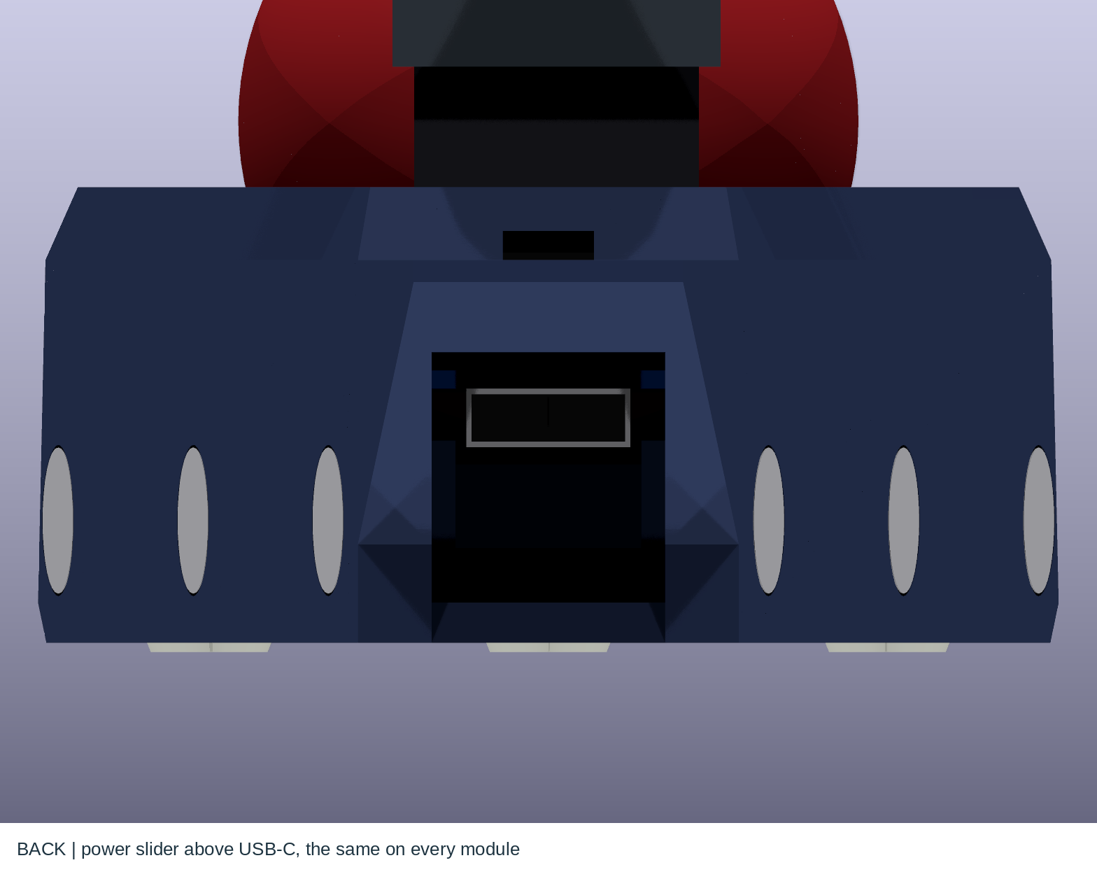
Same switch and same button in the same place on both modules.
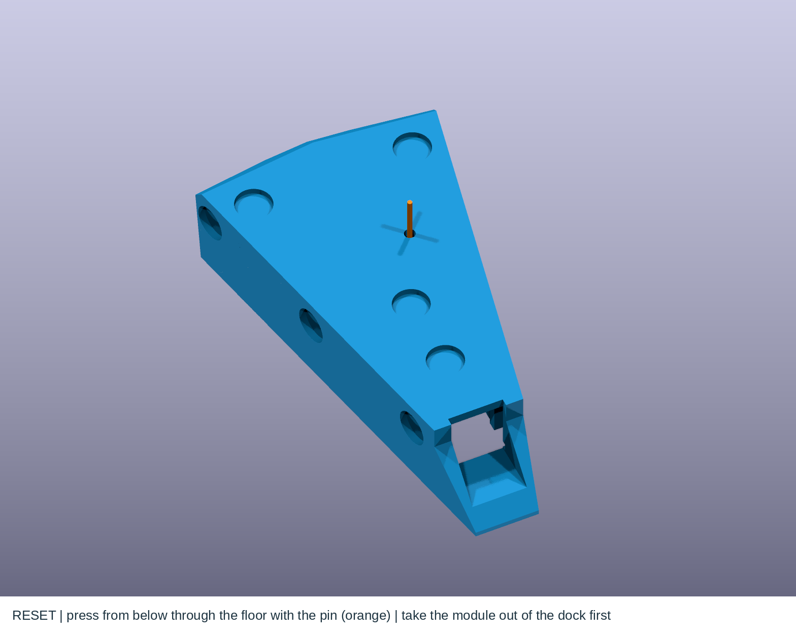
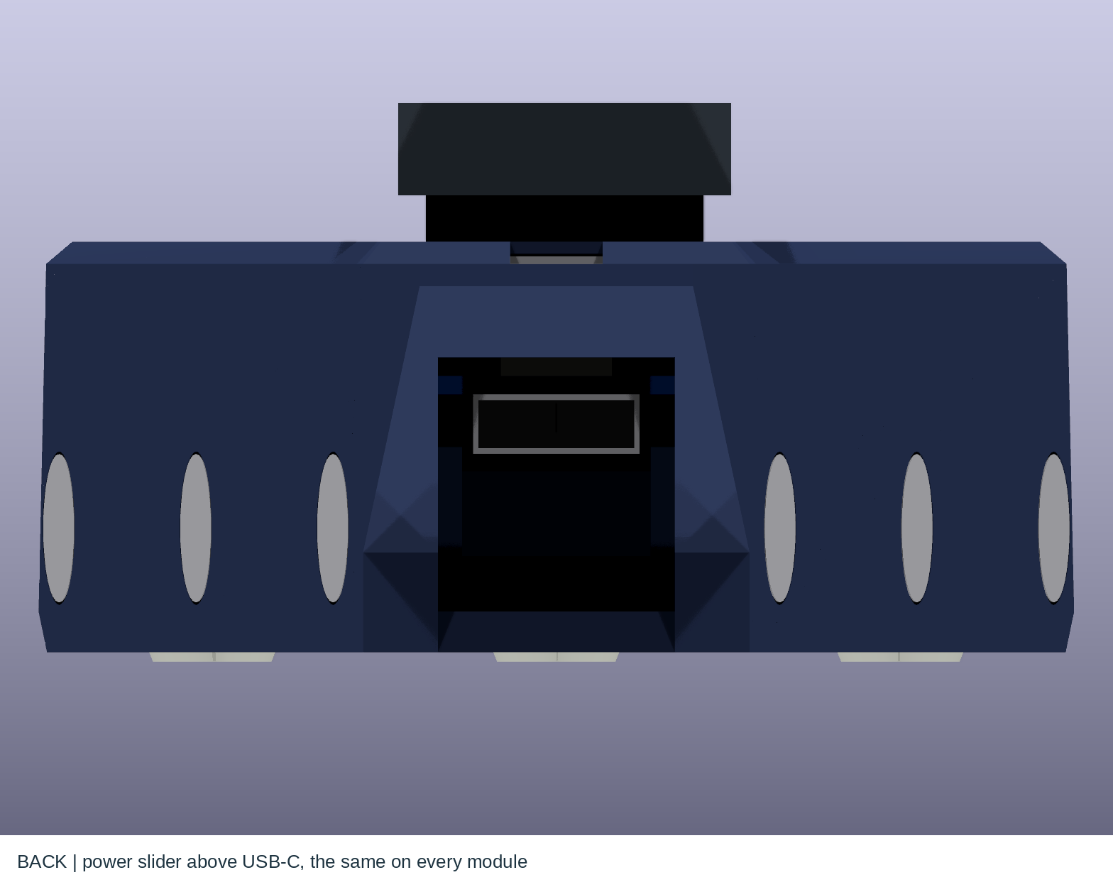
| The power slider, above the USB-C port | Reset, from below |
|---|---|
 |
 |
 |
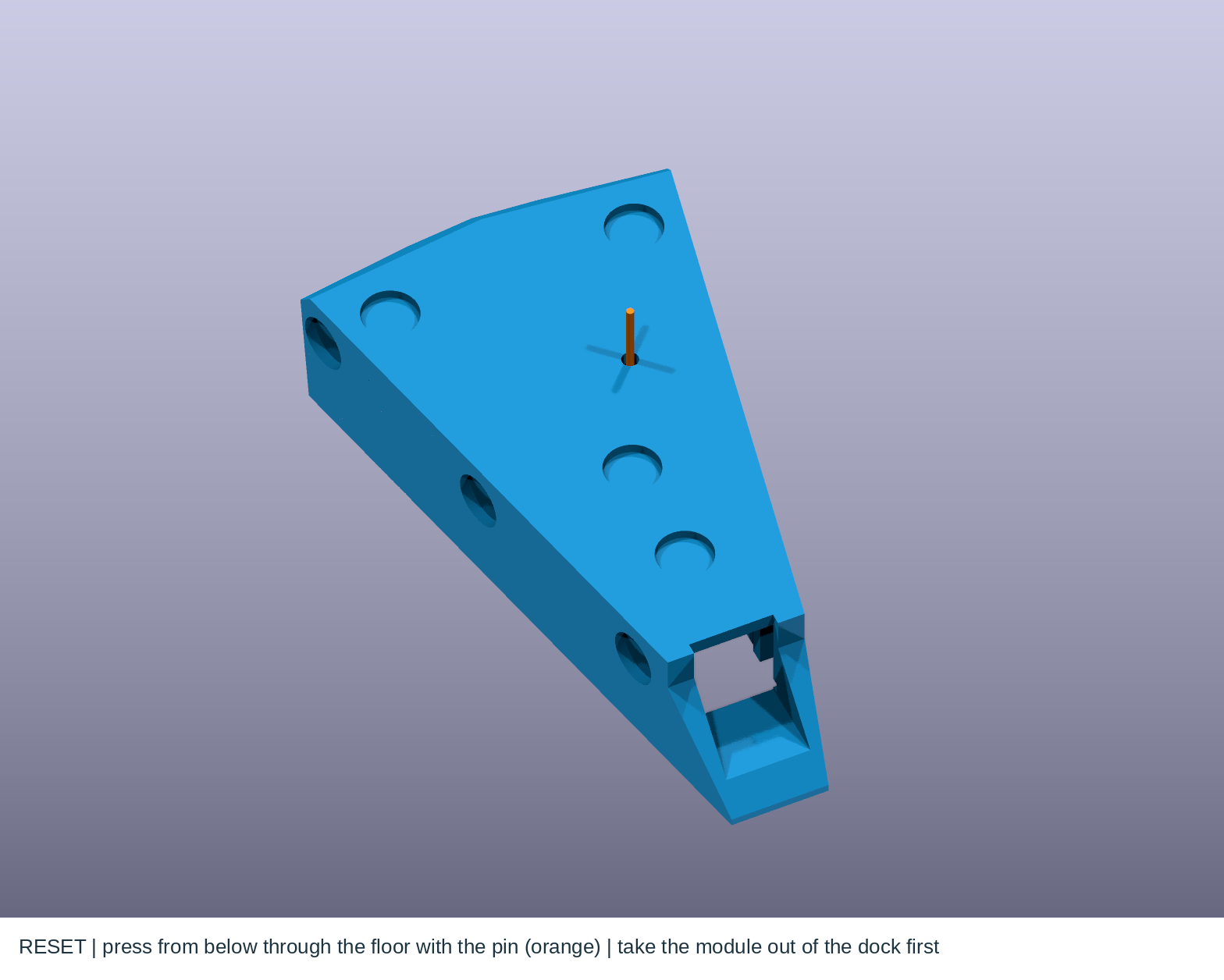 |
The power switch disconnects the battery from both controller and charger: charging requires the switch on. USB can power the controller even with the switch off, so unplug USB, switch off and unsolder the battery's + lead before working on wiring: the module has no battery connector. Use a protected single-cell Li-ion/LiPo pack rated for the controller's charging voltage and current; the main PCB supplies neither a charger nor battery protection. Verify the exact controller's charger, startup/bootloader current settings, battery rating and charge termination under USB load before charging. On a genuine XIAO the selectable charging current is approximately 50 or 100 mA; do not assume a Super52840 uses the same circuit or setting. See Seeed's charging documentation. To reset, take the module out of the dock and press a blunt pin, at most 2 mm across, straight into the hole in the floor: once to reset, twice quickly for the bootloader, if supported by the controller's installed bootloader.
Opening a module
Take it out of the dock, unplug USB, switch it off, and take off the keycaps and ball. Undo the four lid screws and tilt the lid up from the front. The main board stays: it is soldered to the eight stacking pins, so desolder them to take it out. On the trackpad the lid remains attached by the supplied flat cable and the separate DR wire; support it without pulling either, and release the FFC latch if the available slack is insufficient.
Resetting a closed half
Press straight down into the cone above the thumbs with a fingertip (the pad, not the nail, is enough: the cone is 4.2 mm across at the top and the plunger 2.0 mm wide).
- Once: the half reboots.
- Twice quickly: the bootloader. With USB plugged in, a USB drive appears: copy a
.uf2onto it to flash new firmware, as in "Before you start".
Printing
Switch mounts: see SWITCH_MOUNT_RESEARCH.md for the manufacturer drawings and qualification limits. All Choc v1 retaining plates use 1.2 mm thickness, a 2.2 mm PCB-to-plate-top stack and 14.0 mm CAD apertures. The MX lid uses 1.5 mm thickness, a 5.0 mm stack and 14.2 mm CAD apertures. The opening allowances are provisional FDM compensation, not manufacturer tolerances. Measure finished openings and verify both switch clips engage before installing electronics.
- Base: floor-down; intended without supports, subject to bridge inspection in your slicer. The USB recess spans approximately 14.6 mm and pad-slot roofs span 8.6 mm. Inspect bridge direction, anchoring and sag with the intended dry-Nylon profile; add accessible removable support if necessary. For a quiet, solid base, use 4–5 walls and 40–100% infill (gyroid, or solid). More infill means less hollow sound and more weight.
- Plate: top face down: the STL is already oriented that way, with the pillars and screw bosses pointing up. The reset button's cone narrows upwards at 45° from the bed (4.2 mm to 2.8 mm over the first 0.7 mm) and needs no support. Print it solid, at 0.2 mm layers. The switch cutouts are 14.0 mm (13.8 mm + 0.1 mm per side); if your switches are loose or tight, change
cut_tolindesign.pyand regenerate. - Module tray: floor down; the rear hood's underside is designed at 45°. Inspect the 12.8 mm USB bridge and resulting sag clearance to the real plug/controller before assuming support-free printing. Use 4 walls: the screw posts and the 0.9 mm magnet backings carry the load.
- Module lids: top face down; the trackball's cup grows out of the lid as it prints. The intended orientation is support-free.
- Review all module overhangs, particularly the rear hooks, cup and pad ledge, in the actual slicer; support-free printing has not been physically verified. Add removable support if the chosen material and slicer require it, keeping mating surfaces accessible for cleanup.
- Dock: flat side down, with supports inside the stand-base pocket: its roof is at Z = 4.3 mm and has about 5,900 mm² of downward-facing horizontal area. Inspect support-interface material, gap, density, access and removal in the actual slicer. Supports must be removable without damaging the pocket roof, magnet skins or fit surfaces. Measure the cleaned pocket against the actual base; it is not a support-free bridge.
- Fit: nominal allowances include 0.35 mm round a module in the drawer, 0.3 mm round a half on the dock, 0.25 mm round a lid in its tray and 0.15 mm radially round a magnet. These are not guarantees against cumulative print error, warping or elephant foot. Calibrate shrinkage and elephant-foot compensation, and use the same filament and settings for mating parts. Check fits before installing electronics; careful local cleanup may be needed, and a successful first print is not guaranteed.
- Nylon: dry the filament before printing. It's tough enough to take the self-tapping threads without cracking, and its softness damps key noise.
- Release gate: follow PRINT_READINESS.md. Inspect continuous toolpaths through every 0.6–0.9 mm magnet backing/skin, not just the outer mesh. A hypothetical 0.5% error over the 199 mm dock is about 1 mm, greater than the local fit allowances. Measure differential shrinkage and warping of mating parts with the chosen material/profile before a complete build; ±0.2 mm translation tests do not cover either. Never scale just one mating part blindly: that also moves magnets and screw centres. If calibration cannot meet the fit budget, stop and revise/regenerate the geometry.
Everything is a script
One design.json places everything from the key layout: XIAO, battery, connector, screws, magnets. The tent angle is the smallest one the parts under the PCB fit beneath.
Runs headless in the official container. Footprints are written as text and checked against KiCad's library, Seeed's OPL library and kiswitch; the board is then built by script.
Autoroutes the board; pours and stitching vias go on afterwards.
Design-rule check, JLCPCB Gerbers and drill files, and every render on this page.
Builds the base and plate as solids and intersects every part with them. Anything that isn't 0 mm³ fails.
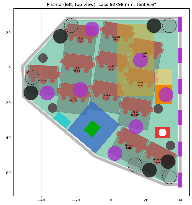
No CAD window, just a loop
A model can't drag parts around in a GUI, so the design lives in code and every judgement is a number or a picture it can inspect.
- GeneratePlacement, footprints, board, solids, all from scripts.
- CheckDRC with zero errors, and the fit check at 0 mm³.
- LookRender the board and case, then read the images.
- Fix upstreamChange the generator, never the output by hand.
- RegenerateRerun the whole chain from
design.py.
What gets checked
Every part that could collide is modelled, and the fit check fails on anything above 0 mm³. Some checks cover how the keyboard is assembled and used, not only where parts sit:
A USB-C cable seats fully
A recess the size of the largest Type-C overmold (12.35 × 6.5 mm) reaches the port, and the PCB edge is notched in front of it. The check plugs in a cable of that size.
The PCB drops straight in
The power switch's lever reaches past the PCB edge, so it slides down a slot open to the top, wider outwards so a fingernail reaches the lever. The check sweeps the lever along the drop-in path.
Room for tolerances
0.5 mm around the PCB and plate covers JLCPCB's ±0.2 mm outline tolerance plus print shrinkage.
One magnet throughout
Thirteen 8 × 1.5 mm N52 discs per half: six along the seam and seven underneath, three of them stand contacts. Each pocket keeps 0.5 mm of plastic all round, measured against the printed base. The 500 mAh battery raises the PCB and case by 1.8 mm without changing the PCB outline or wiring.
$ python check_fit.py
sockets vs base                       0.000 mm3
xiao vs base                          0.000 mm3
battery vs sockets                    0.000 mm3
plate vs base                         0.000 mm3
usb plug vs base                      0.000 mm3
usb plug vs pcb                       0.000 mm3
switch lever (dropping in) vs base    0.000 mm3
reset button body vs plate            0.000 mm3
seam magnet 1 (+0.5 all round) vs voids    0.000 mm3
magnets (+0.5) vs each other          0.000 mm3
stacked: left pads vs right pads      0.000 mm3
balance, unibody      nearest key  2.79 mm inside (2.0 needed): ok
ALL CLEAR
Excerpt of the output.